CIGS thin film assembly of solar unmanned aerial vehicle and internal-external cascading method thereof
A technology of solar drones and thin-film modules, which is applied in electrical components, semiconductor devices, photovoltaic power generation, etc., can solve the problems of low open circuit voltage and loop loss, and achieve high open circuit voltage, small output current, and small current internal resistance loss Effect
- Summary
- Abstract
- Description
- Claims
- Application Information
AI Technical Summary
Problems solved by technology
Method used
Image
Examples
specific Embodiment 1
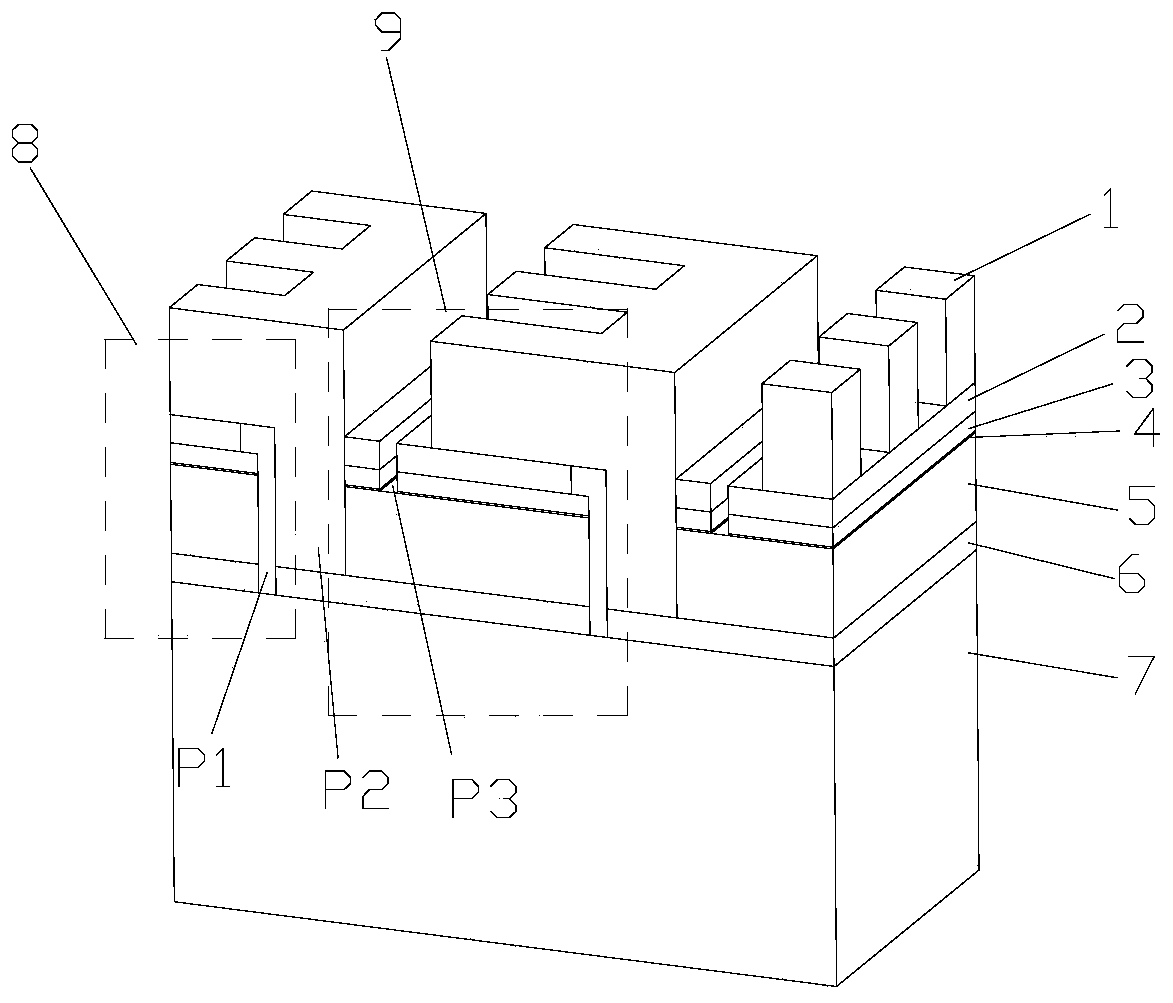
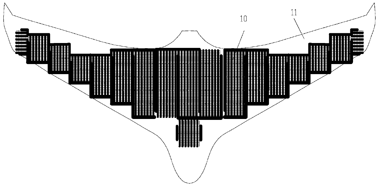
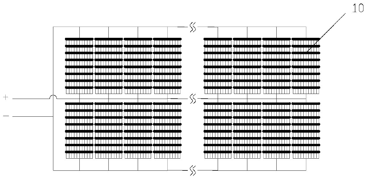
[0054] Firstly, through three picosecond laser scribing lines, the thin-film solar cell material layers from the transparent conductive layer 2 to the Mo back electrode layer 6, the ZnO window layer 3 to the CIGS absorbing layer 5, and the ZnO window layer 3 to the top electrode 1 are selectively transferred. In addition, the grooves of P1 scribe, P2 scribe, and P3 scribe are formed, wherein the P1 scribe channel has a width of about 50 μm and a depth of about 4 μm, and a P2 scribe channel has a width of about 200 μm and a depth of about 3.1 μm. , the width of the P3 scribed channel is about 50 μm, and the depth is about 0.6 μm; add insulating paste and conductive paste to the P1 scribed channel and P2 scribed channel respectively to realize the series connection between sub-cells; figure 2 As shown, the monolithically integrated battery cells are welded in parallel with bus bars; the final assembly is laminated and packaged. Specific steps are as follows:
[0055] (1) Laser...
specific Embodiment 2
[0068] Such as figure 1 As shown, three picosecond laser scribing lines are used to separate the thin-film solar cell material layers from the transparent conductive layer 2 to the Mo back electrode layer 6, from the ZnO window layer 3 to the CIGS absorber layer 5, and from the ZnO window layer 3 to the top electrode 1. Selective removal to form channels for P1 scribe, P2 scribe, P3 scribe,
[0069] Among them, the width of the P1 scribed channel is about 24 μm, and the depth is about 4 μm; the width of the P2 scribed channel is about 46 μm, and the depth is about 3.1 μm; the width of the P3 scribed channel is about 100 μm, and the depth is about 3.1 μm; Add insulating paste and conductive paste to P1 scribed channel and P2 scribed channel respectively to realize the series connection between sub-batteries; figure 2 As shown, the monolithically integrated battery cells are welded in parallel with bus bars; the final assembly is laminated and packaged. Specific steps are as ...
PUM
| Property | Measurement | Unit |
|---|---|---|
| thickness | aaaaa | aaaaa |
| thickness | aaaaa | aaaaa |
| thickness | aaaaa | aaaaa |
Abstract
Description
Claims
Application Information


