A method and system for measuring pn junction depth of indium antimonide material

An indium antimonide, PN junction technology, applied in semiconductor/solid-state device testing/measurement, electrical components, circuits, etc., can solve the problems of complex process implementation, long cycle, long process time, etc., to simplify the measurement operation process, reduce Measurement cost, simple operation effect

Active Publication Date: 2021-09-03
11TH RES INST OF CHINA ELECTRONICS TECH GROUP CORP
View PDF5 Cites 0 Cited by
  • Summary
  • Abstract
  • Description
  • Claims
  • Application Information

AI Technical Summary

Problems solved by technology

However, the first scheme uses a secondary ion mass spectrometer for testing. Due to the expensive equipment, only a few research institutes in China have purchased this equipment, so the PN junction measurement has the problems of high price, long cycle, and inconvenient; while the second scheme In the plan, the method of grinding and oxidation is used for testing, which involves the grinding and polishing thinning process of the device. The process is complicated to realize, and the design of multiple process operations and the use of various chemical reagents require a long process time.

Method used


Image

  • A method and system for measuring pn junction depth of indium antimonide material
  • A method and system for measuring pn junction depth of indium antimonide material
  • A method and system for measuring pn junction depth of indium antimonide material

Examples


Embodiment Construction

[0049] In order to further explain the technical means and functions adopted by the present invention to achieve the intended purpose, the present invention will be described in detail below in conjunction with the accompanying drawings and preferred embodiments.

[0050] First, some terms involved in the embodiments of the present invention are described to facilitate the understanding of those skilled in the art.

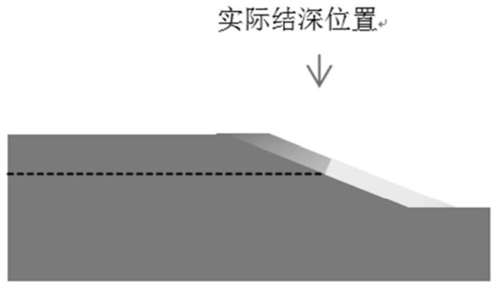
[0051] PN junction: Different doping processes are used to combine P-type semiconductors (P is the prefix of Positive, which is named because the holes are positively charged) and N-type semiconductors (N is the prefix of Negative, due to the effect of diffusion) Electrons are negatively charged to get this name) are fabricated on the same semiconductor (usually silicon or germanium) substrate, and a space charge region is formed at their interface called a PN junction. The PN junction has unidirectional conductivity, which is a characteristic used by many devices...


PUM


Abstract

The invention provides a method and system for measuring the PN junction depth of an indium antimonide material, which is used to simplify the process of measuring the PN depth of the indium antimonide material and reduce the measurement cost. The method for measuring the PN junction depth of the indium antimonide material includes: immersing the indium antimonide material with the PN junction structure in an etchant and corroding to form a corrosion slope; placing the indium antimonide material after etching in deionized water for cleaning and drying Place the dried indium antimonide material in an anodizing device for anodic oxidation until the surface of the corrosion slope has different colors to form two color areas; place the oxidized indium antimonide material in deionized water for cleaning and drying ; According to the boundary of the surface color of the corroded slope, measure the first width of the corroded slope and the second width of the color partition of the corroded slope top respectively; Utilize a step meter to measure the height of the corroded slope; The second width and the height of the corrosion slope determine the depth of the PN junction.

Description

technical field [0001] The invention relates to the technical field of semiconductors, in particular to a method and a system for measuring the depth of a PN junction of an indium antimonide material. Background technique [0002] Indium antimonide material is the mainstream material for the preparation of mid-wave infrared detectors. After diffusion, ion implantation or epitaxy, a PN junction structure is formed. After passivation, electrodes, flip-chip interconnection and other processes in the later stage, a detector chip is prepared. The tiles are packaged into detector components and can be used in various fields of sea, land and air to realize night vision, tracking and other functions. In the infrared detector process, the quality of PN junction preparation is the core to determine the final performance index of the detector. The junction depth of the PN junction directly affects the main performance indicators of the detector, such as quantum efficiency, detection ra...

Claims


Application Information

Patent Timeline
Patent Type & Authority Patents(China)
IPC IPC(8): H01L21/66
CPCH01L22/12
Inventor 邱国臣李海燕
Owner 11TH RES INST OF CHINA ELECTRONICS TECH GROUP CORP
Why Eureka
Try Eureka