Semiconductor ultraviolet photoelectric detector

A technology for photodetectors and electrical detectors, which is applied in semiconductor devices, electrical solid state devices, circuits, etc., and can solve problems such as bulky volume and high price.

Inactive Publication Date: 2020-01-10
SHENZHEN INST OF WIDE BANDGAP SEMICON
View PDF4 Cites 4 Cited by
  • Summary
  • Abstract
  • Description
  • Claims
  • Application Information

AI Technical Summary

Problems solved by technology

In addition, ultraviolet photodetectors in the form of discrete devices require subsequent signal amplifica

Method used


Image

  • Semiconductor ultraviolet photoelectric detector
  • Semiconductor ultraviolet photoelectric detector
  • Semiconductor ultraviolet photoelectric detector

Examples


preparation example Construction

[0029] The preparation method of the proposed semiconductor ultraviolet photodetector, the specific steps are:

[0030] (1) Prepare semiconductor ultraviolet photodetector epitaxial structure, including figure 1 The substrate (10) shown, the gallium nitride layer (9) and aluminum gallium nitride (7) epitaxially grown on the substrate;

[0031] (2) Photolithography and etching define the AlGaN region (7) of the Schottky photodetector and the AlGaN region (8) of the high electron mobility transistor;

[0032] (3) photolithography, etching and depositing metal to form the source (5) and drain (6) of the high electron mobility transistor;

[0033] (4) high temperature annealing to form ohmic contacts;

[0034] (5) photoetching and depositing metal to form the control gate (3) and the electrical suspension gate (4) of the photodetector and transistor suspension gate;

Embodiment 1

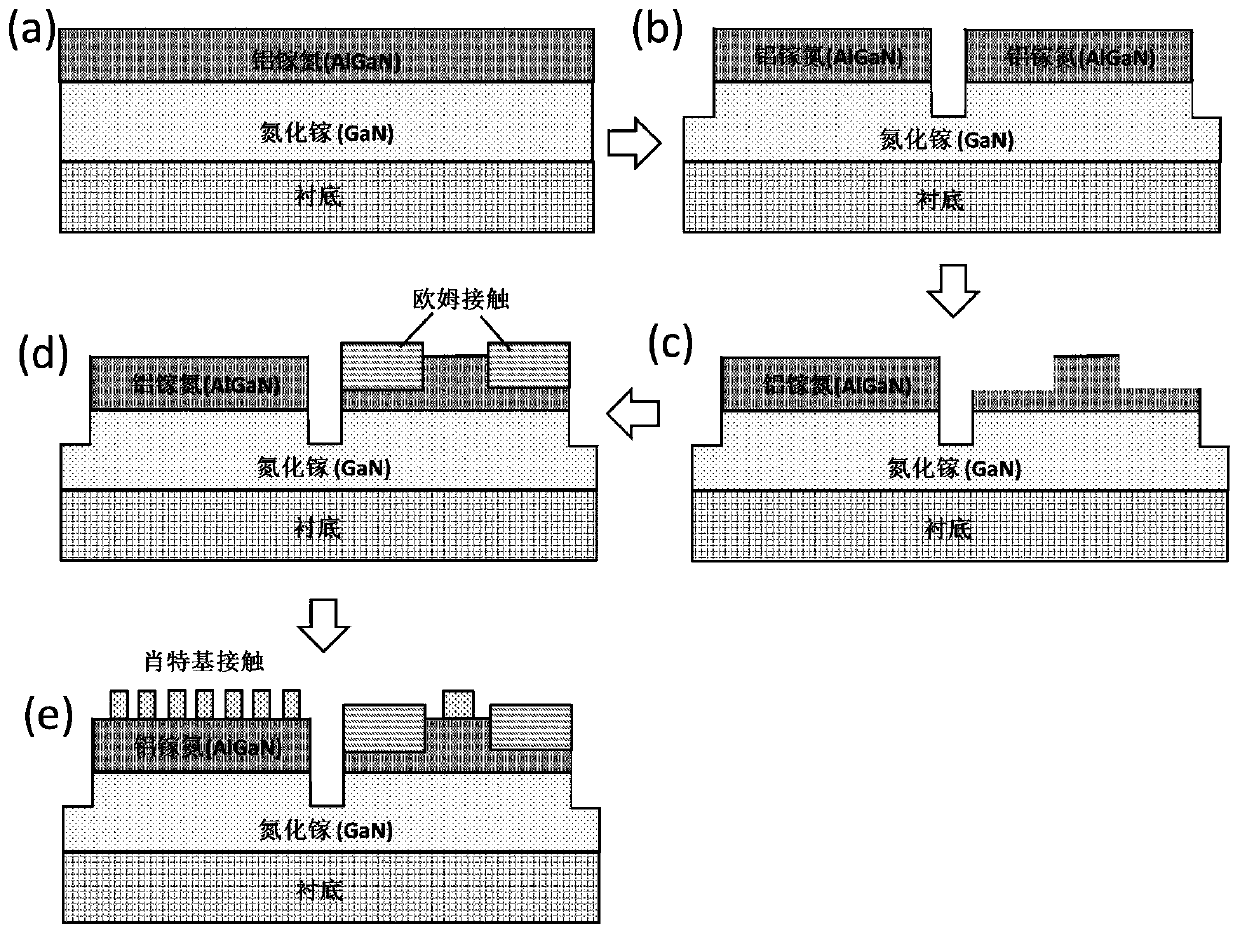
[0037] Embodiment 1 (corresponding figure 1 device structure and figure 2 process flow):

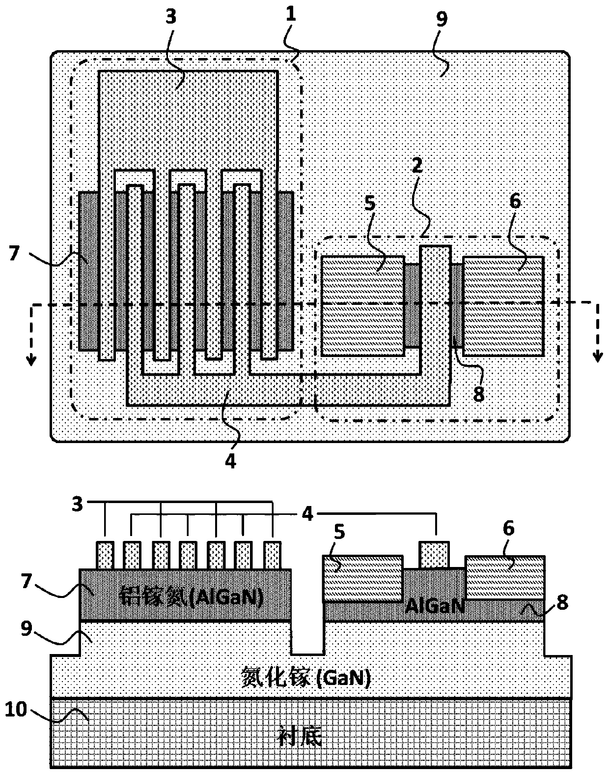
[0038] The semiconductor ultraviolet photodetector proposed by the present invention combines the ultraviolet photodetection of the Schottky junction and the high electron mobility transistor, and its device structure is as follows figure 1 As shown, it consists of two parts: a Schottky photodetector (1) and a high electron mobility transistor (2) for signal amplification. The specific structure includes the control gate (3), the electrical floating gate (4), the source (5) and drain (6) ohmic contacts of the high electron mobility transistor, the AlGaN region of the Schottky photodetector ( 7) and the AlGaN region (8) of the high electron mobility transistor, the GaN buffer / channel layer (9) and the substrate for epitaxy (10).

[0039] (1) if figure 2 (a) shows the starting base, including the substrate, the epitaxial GaN channel layer and the uppermost AlGaN layer. The substrate...

Embodiment 2

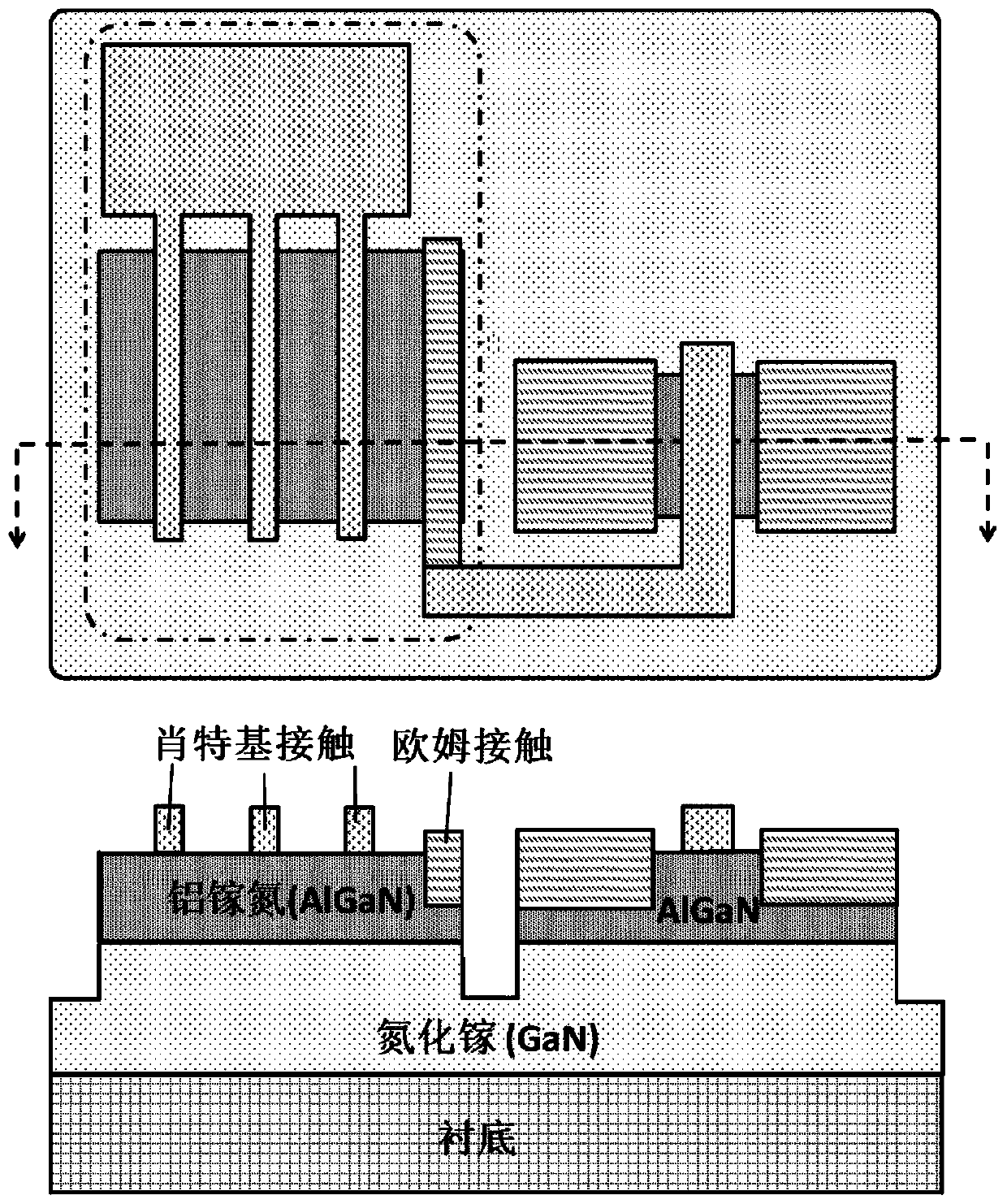
[0043] Embodiment 2 (corresponding image 3 device structure diagram)

[0044] Embodiment 2 is similar to Embodiment 1, except that the structure of the Schottky photodetector is slightly different. In this embodiment, the floating gate uses an ohmic contact to replace the Schottky contact. Thus, a single Schottky junction of metal / semiconductor contact is formed in the AlGaN layer between the Schottky gate and the two-dimensional electron gas, and Not the metal / semiconductor / metal dual Schottky structure in Example 1. This embodiment is combined with reducing the number of metal interdigitated electrodes, thereby increasing light transmittance and detection sensitivity. The difference in the specific implementation method is that the floating gate is implemented in step (3) by using an ohmic contact. However, the gate of the high electron mobility transistor is still formed by a Schottky contact in step (4).


PUM

PropertyMeasurementUnit
Thicknessaaaaaaaaaa
Total thicknessaaaaaaaaaa

Abstract

The invention belongs to the field of semiconductor devices, and particularly relates to a high-sensitivity integrated semiconductor ultraviolet photoelectric detector. A reversely biased Schottky junction converts incident photons into photoelectrons. Generated photoelectrons are accumulated on an electrically suspended gate, the breakover current of a high-electron-mobility transistor is regulated and controlled, and therefore photo-induced electrons are amplified, and high detection sensitivity is achieved. Compared with a common independent ultraviolet photoelectric detector, the device provided by the invention has two advantages that a photoelectric signal is amplified by utilizing the high-electron-mobility transistor, so that the sensitivity is greatly improved; the ultraviolet photoelectric detection Schottky diode and the high-electron-mobility transistor are integrated on the same substrate, so that a multifunctional monolithic integration module can be formed, and the sizeand the cost of the system can be reduced.

Description

technical field [0001] The invention belongs to the technical field of semiconductor devices, in particular to a semiconductor ultraviolet photodetector. Background technique [0002] Photodetectors working in the ultraviolet band, especially in the wavelength range of 200nm-280nm, have unique advantages and applications. In solar radiation, ultraviolet rays with wavelengths in the range of 200nm-280nm are strongly absorbed by the ozone layer, and the background radiation reaching the surface is very small, which is called "solar-blind ultraviolet region". The "sun-blind ultraviolet" photodetector working in this band is less disturbed by the background noise of the sun, and has a wide range of uses in the military and civilian fields. Solar-blind ultraviolet photodetectors can be used in arc discharge detection in power systems, missile early warning, fire monitoring and space exploration and other fields. Compared with visible light and infrared detectors, it has the adv...

Claims


Application Information

Patent Timeline
IPC IPC(8): H01L27/146H01L31/18
CPCH01L27/14612H01L27/14689H01L31/1848Y02P70/50
Inventor 万景刘冉叶怀宇张国旗
Owner SHENZHEN INST OF WIDE BANDGAP SEMICON
Why Eureka
Try Eureka