P-type tunneling oxide passivation contact solar cell and preparation method thereof
A technology of solar cells and oxides, applied in circuits, photovoltaic power generation, electrical components, etc., can solve the problems of reducing the conversion efficiency of cells, affecting the effect of passivation, and reducing the passivation ability, achieving excellent interface passivation effect, reducing The effect of compounding speed and high conversion efficiency
- Summary
- Abstract
- Description
- Claims
- Application Information
AI Technical Summary
Problems solved by technology
Method used
Image
Examples
Embodiment 1
[0036] A method for preparing a P-type tunnel oxide passivation contact solar cell, comprising the following steps:
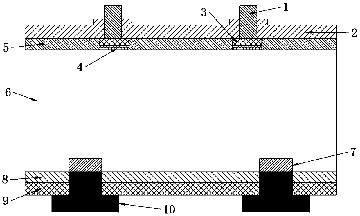
[0037] (S1), using alkali texture, P-type silicon 6 is placed in the groove to remove the damaged layer and texture, forming a 0.5 μm high pyramid texture;
[0038] (S2), using phosphorus oxychloride POCl 3 Carry out high-temperature diffusion, the reaction temperature is 750°C, and the reaction time is 30 minutes, and an N-type heavily doped silicon layer 5 is formed on the surface of the P-type silicon 6;
[0039] (S3), using HF solution to remove the phosphosilicate glass layer PSG on the surface of the P-type silicon 6;
[0040] (S4), using the RCA wet chemical method to clean the surface of the silicon wafer;
[0041] (S5), use low-pressure chemical vapor deposition (LPCVD) or plasma-enhanced chemical vapor deposition (PECVD) to form a silicon dioxide layer 4 on the front of the P-type silicon 6, and the thickness of the N-type heavily doped polysilicon la...
Embodiment 2
[0049] A method for preparing a P-type tunnel oxide passivation contact solar cell, comprising the following steps:
[0050] (S1), using alkali texture, P-type silicon 6 is placed in the groove to remove the damaged layer and texture, forming a 5 μm high pyramid texture;
[0051] (S2), using phosphorus oxychloride POCl 3 Carry out high-temperature diffusion, the reaction temperature is 850°C, and the reaction time is 60 minutes, and an N-type heavily doped silicon layer 5 is formed on the surface of the P-type silicon 6;
[0052] (S3), using HF solution to remove the phosphosilicate glass layer PSG on the surface of the P-type silicon 6;
[0053] (S4), using the RCA wet chemical method to clean the surface of the silicon wafer;
[0054] (S5), use low-pressure chemical vapor deposition (LPCVD) or plasma-enhanced chemical vapor deposition (PECVD) to form a silicon dioxide layer 4 on the front of the P-type silicon 6, and the thickness of the N-type heavily doped polysilicon la...
Embodiment 3
[0062] A method for preparing a P-type tunnel oxide passivation contact solar cell, comprising the following steps:
[0063] (S1), using alkali texture, P-type silicon 6 is placed in the groove to remove the damaged layer and texture, forming a 2 μm high pyramid texture;
[0064] (S2), using phosphorus oxychloride POCl 3 Carry out high-temperature diffusion, the reaction temperature is 800°C, and the reaction time is 50 minutes, and an N-type heavily doped silicon layer 5 is formed on the surface of the P-type silicon 6;
[0065] (S3), using HF solution to remove the phosphosilicate glass layer PSG on the surface of the P-type silicon 6;
[0066] (S4), using the RCA wet chemical method to clean the surface of the silicon wafer;
[0067] (S5), use low-pressure chemical vapor deposition (LPCVD) or plasma-enhanced chemical vapor deposition (PECVD) to form a silicon dioxide layer 4 on the front of the P-type silicon 6, and the thickness of the N-type heavily doped polysilicon la...
PUM
| Property | Measurement | Unit |
|---|---|---|
| Thickness | aaaaa | aaaaa |
| Thickness | aaaaa | aaaaa |
| Thickness | aaaaa | aaaaa |
Abstract
Description
Claims
Application Information
 - R&D
- Intellectual Property
- Life Sciences
- Materials
- Tech Scout
- Unparalleled Data Quality
- Higher Quality Content
- 60% Fewer Hallucinations
Browse by: Latest US Patents, China's latest patents, Technical Efficacy Thesaurus, Application Domain, Technology Topic, Popular Technical Reports.
© 2025 PatSnap. All rights reserved.Legal|Privacy policy|Modern Slavery Act Transparency Statement|Sitemap|About US| Contact US: help@patsnap.com


