

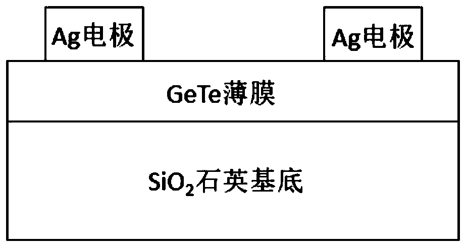
Ultra-wideband thin film photoelectric detector and preparation method thereof
A photodetector and ultra-wideband technology, which is applied in the direction of electrical components, semiconductor devices, circuits, etc., can solve problems such as the inability to realize photoelectric detection, achieve high yield, high response value, and improve the effect of photocurrent density
- Summary
- Abstract
- Description
- Claims
- Application Information
AI Technical Summary
Problems solved by technology
Method used
Image

Examples
Embodiment 1
[0072] The preparation method is as follows:
[0073] (1) Select insulating SiO 2 Quartz substrate;
[0074] (2) SiO 2 The quartz substrate was ultrasonically cleaned in alcohol, acetone and deionized water for 60 seconds; after taking it out, it was blown dry with high-purity nitrogen;
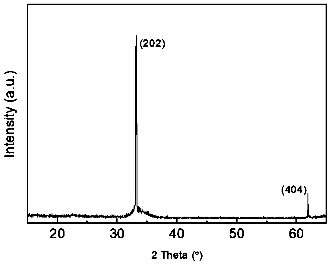
[0075] (3) Rinse the above-mentioned SiO with deionized water and dry it with high-purity nitrogen 2 The quartz substrate is loaded into the tray and put into the vacuum chamber, and the vacuum chamber is evacuated to 5×10 -4 Pa, the SiO 2 The temperature of the quartz substrate was adjusted to the first temperature of 450°C, the pressure of the argon gas was adjusted to the first pressure of 1.0Pa, and the DC magnetron sputtering technology was used to bombard the GeTe target with ionized ions. 2 On the surface of the quartz substrate, a layer of 300nm GeTe film layer is deposited;
[0076] (4) After the deposition is completed, at 3×10 -4 Under Pa vacuum conditions, the sample temper...
Embodiment 2
[0081] The base heating temperature (first temperature) in embodiment 1 is 300 ℃;
[0082] All the other are the same as in Example 1.
[0083] After testing, the prepared Ag-GeTe-Ag photodetection device has no photodetection performance for incident light in any wavelength band.
Embodiment 3
[0085] The base heating temperature (first temperature) in embodiment 1 is 400 ℃;
[0086] All the other are the same as in Example 1.
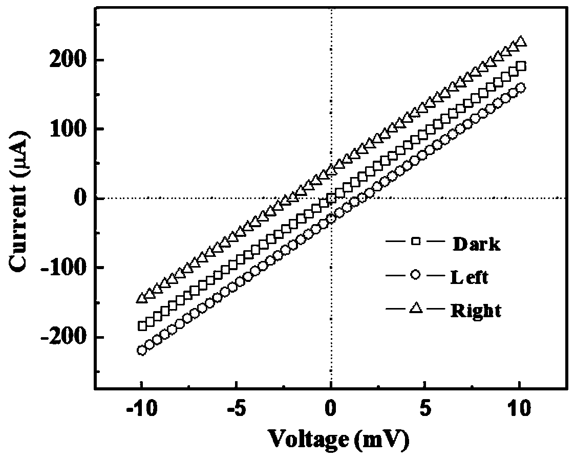
[0087] After testing, the prepared Ag-GeTe-Ag photodetection device has weak light detection performance in the wavelength range of 404nm-10μm: when the wavelength λ=404nm, the responsivity is 0.1A / W; when λ=1550nm, The responsivity is 0.08A / W; when λ=10μm, the responsivity is 0.13A / W.
PUM
| Property | Measurement | Unit |
|---|---|---|
| thickness | aaaaa | aaaaa |
| thickness | aaaaa | aaaaa |
| thickness | aaaaa | aaaaa |
Abstract
Description
Claims
Application Information