Fabrication method of mesa photodetector

A technology for photodetectors and manufacturing methods, applied in circuits, electrical components, semiconductor devices, etc., can solve the problems affecting device responsivity, dark current, quantum efficiency reliability and operating speed, increase surface recombination rate and surface leakage current , surface oxidation and other issues, to achieve the effect of reducing the probability of formation, reducing dark current, and high performance

Active Publication Date: 2020-12-22
武汉敏芯半导体股份有限公司
View PDF10 Cites 0 Cited by
  • Summary
  • Abstract
  • Description
  • Claims
  • Application Information

AI Technical Summary

Problems solved by technology

Its disadvantage is that in the process of glue removal and subsequent cleaning and leveling, the photosensitive surface structure on the top of the mesa photodetector will be exposed for a long time, which will cause problems such as surface oxidation and the introduction of unnecessary impurities, resulting in the formation of A large number of surface states will increase the surface recombination rate and surface leakage current, etc., which will seriously affect the performance indicators of the device such as responsivity, dark current, quantum efficiency, reliability and operating speed

Method used


Image

  • Fabrication method of mesa photodetector
  • Fabrication method of mesa photodetector
  • Fabrication method of mesa photodetector

Examples


Embodiment Construction

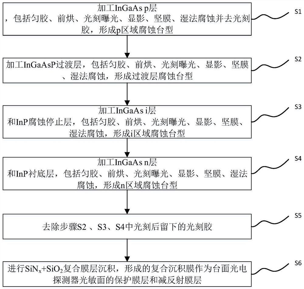
[0066] In order to make the object, technical solution and advantages of the present invention clearer, the present invention will be further described in detail below in conjunction with the accompanying drawings and embodiments. It should be understood that the specific embodiments described here are only used to explain the present invention, not to limit the present invention.

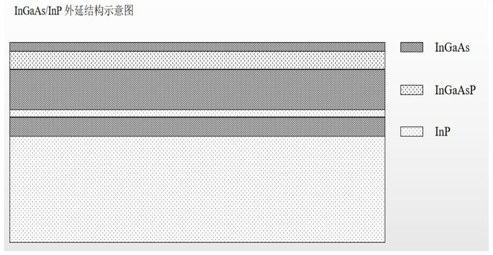
[0067] The epitaxial structure of the mesa-type InGaAs / InP PIN photodetector processed in the embodiment of the present invention is as attached figure 2 As shown, from top to bottom are:

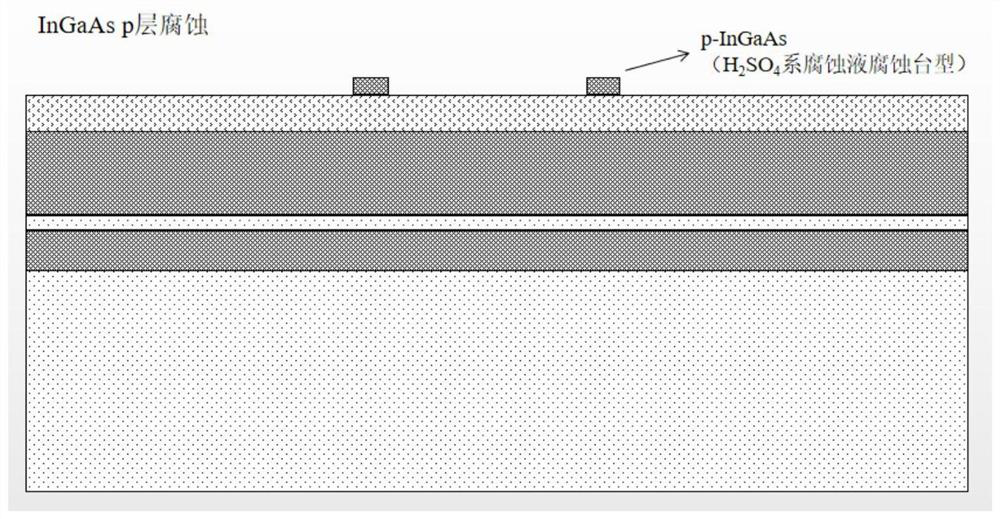
[0068] (1) InGaAs layer, PIN structure p layer, thickness is about 0.1-0.3 μm.

[0069] (2) InGaAsP layer, a transition layer, with a thickness of about 0.3-0.5 μm.

[0070] (3) InGaAs layer, i-layer of PIN structure, with a thickness of about 2-3 μm.

[0071] (4) InP layer, the corrosion stop layer, the thickness is about 30nm.

[0072] (5) InGaAs layer, an n-layer of PIN structure, with a thickness of abo...


PUM

PropertyMeasurementUnit
thicknessaaaaaaaaaa
thicknessaaaaaaaaaa
thicknessaaaaaaaaaa

Abstract

The invention discloses a manufacturing method of a mesa type photoelectric detector. According to the manufacturing method, in the process of processing the InGaAsP transition layer, the InGaAs i layer, the InP corrosion stopping layer, the InGaAs n layer and the InP substrate layer, photoresist removing treatment is not carried out, and finally photoresist left after photoetching is removed at atime. According to the invention, the gluing layer is used for fully protecting the photosensitive surface structure of the photoelectric detector; the InGaAs / InP PIN mesa photoelectric detector withhigh performance is obtained by removing photoresist, cleaning the InGaAs / InP PIN mesa photoelectric detector, avoiding bringing new impurities and contact oxidation with oxygen in the steps of photoresist removal, cleaning and the like, reducing the formation probability of the surface state of the device, and reducing the dark current of the device.

Description

technical field [0001] The invention belongs to the technical field of photodetector chip manufacturing and processing, and relates to a method for manufacturing and processing a mesa-shaped photoelectric detector. Background technique [0002] Modern society is a highly informationized society. As the main way of information transmission, optical fiber communication is developing rapidly towards ultra-high speed and large capacity. 5G brings new opportunities and challenges to the development of optical fiber communication. Whether it is optical fiber, optical module, optical access network system, etc., the entire industry needs technological innovation and application breakthrough. Photodetectors are one of the important devices in optical communication systems. They can convert optical signals into electrical signals for signal processing. The advent of the 5G era puts forward higher requirements on the performance of optical detectors. [0003] Early photodiodes consi...

Claims


Application Information

Patent Timeline
Patent Type & Authority Patents(China)
IPC IPC(8): H01L31/18H01L31/105
CPCH01L31/105H01L31/1844Y02P70/50
Inventor 余沛王丹王权兵徐之韬
Owner 武汉敏芯半导体股份有限公司
Why Eureka
Try Eureka