Light emitting diode epitaxial wafer and manufacturing method thereof

A technology for light-emitting diodes and manufacturing methods, which is applied to electrical components, circuits, semiconductor devices, etc., can solve the problems of large compressive stress of InGaN layers and GaN layers, affecting LED luminous efficiency, and decreasing internal quantum efficiency, so as to improve interface quality, The effect of improving the band tilt phenomenon and improving the internal quantum efficiency

Active Publication Date: 2020-01-21
HC SEMITEK ZHEJIANG CO LTD
View PDF10 Cites 11 Cited by
  • Summary
  • Abstract
  • Description
  • Claims
  • Application Information

AI Technical Summary

Problems solved by technology

However, there is a large lattice mismatch between the InGaN layer and the GaN layer, resulting in a large compressive stress between the InGaN layer and the GaN layer
Compressive stress will generate a piezoelectric polarization electric field, which reduces the overlap of electron and hole wave functions, resulting in a tilt of the energy band of the multi-quantum well layer, resulting in a decrease in internal quantum efficiency, thereby affecting LED luminous efficiency.

Method used


Image

  • Light emitting diode epitaxial wafer and manufacturing method thereof
  • Light emitting diode epitaxial wafer and manufacturing method thereof
  • Light emitting diode epitaxial wafer and manufacturing method thereof

Examples


Embodiment Construction

[0029] In order to make the object, technical solution and advantages of the present invention clearer, the implementation manner of the present invention will be further described in detail below in conjunction with the accompanying drawings.

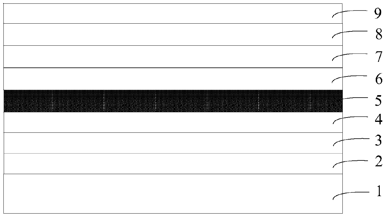
[0030] An embodiment of the present invention provides a light emitting diode epitaxial wafer, figure 1 It is a schematic structural diagram of a light-emitting diode epitaxial wafer provided by an embodiment of the present invention, as shown in figure 1 As shown, the light-emitting diode epitaxial wafer includes a substrate 1, a buffer layer 2, an undoped GaN layer 3, an N-type layer 4, a multi-quantum well layer 5, a low-temperature P-type layer 6, Electron blocking layer 7 , high temperature P-type layer 8 and P-type contact layer 9 .

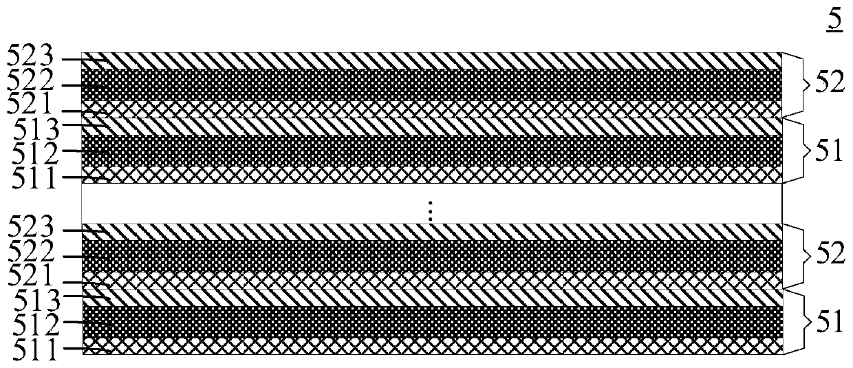
[0031] figure 2 is a schematic structural diagram of a multi-quantum well layer provided by an embodiment of the present invention, such as figure 2 As shown, the multiple quantum well layer 5 ...


PUM

PropertyMeasurementUnit
thicknessaaaaaaaaaa
thicknessaaaaaaaaaa
thicknessaaaaaaaaaa

Abstract

The invention discloses a light emitting diode epitaxial wafer and a manufacturing method thereof, and belongs to the semiconductor technology field. Each quantum well layer of a multi-quantum well layer of the light-emitting diode epitaxial wafer comprises a first quantum well sub-layer, a second quantum well sub-layer and a third quantum well sub-layer which are stacked in sequence. In / Ga ratioof the second quantum well sub-layer is greater than or equal to the In / Ga ratios of the first quantum well sub-layer and the third quantum well sub-layer. Si is doped in the first quantum well sub-layer. Each quantum barrier layer comprises a first quantum barrier sub-layer, a second quantum barrier sub-layer and a third quantum barrier sub-layer which are stacked in sequence. The Si / Ga ratio ofthe second quantum barrier sub-layer is greater than or equal to the Si / Ga ratios of the first quantum barrier sub-layer and the third quantum barrier sub-layer. The light emitting diode epitaxial wafer can improve an energy band inclination phenomenon in the multi-quantum well layer, an overlapping degree of wave functions of electrons and holes in space distribution is increased and internal quantum efficiency of an LED is improved.

Description

technical field [0001] The invention relates to the technical field of semiconductors, in particular to a light-emitting diode epitaxial wafer and a manufacturing method thereof. Background technique [0002] GaN (gallium nitride) is one of the materials for making LED (Light Emitting Diode, light-emitting diode) epitaxial wafers. GaN is an extremely stable compound and a hard high-melting point material. It is also a direct transition wide-bandgap semiconductor material. It not only has good Physical and chemical properties, but also has a high electron saturation rate. Good thermal conductivity, large bandwidth and small dielectric constant and strong anti-radiation ability can be used to prepare high-power devices with good stability, long life, corrosion resistance and high temperature resistance. [0003] Typically, GaN-based LEDs are epitaxially grown on sapphire substrates. The traditional GaN-based LED epitaxial structure generally uses the InGaN / GaN superlattice s...

Claims


Application Information

Patent Timeline
Patent Type & Authority Applications(China)
IPC IPC(8): H01L33/06H01L33/12H01L33/32H01L33/00
CPCH01L33/0066H01L33/0075H01L33/06H01L33/12H01L33/325
Inventor 洪威威王倩周飚胡加辉
Owner HC SEMITEK ZHEJIANG CO LTD
Why Eureka
Try Eureka