Method for growing gallium nitride film on silicon substrate

A gallium nitride and silicon substrate technology, applied in electrical components, nanotechnology, semiconductor/solid-state device manufacturing, etc., can solve problems such as large differences in lattice constant and thermal expansion coefficient, large tensile stress, cracks, etc., to prevent The effect of melting back etching reaction, eliminating surface cracks and alleviating lattice mismatch

Inactive Publication Date: 2020-02-04
BEIJING HUAJINCHUANGWEI ELECTRONICS CO LTD +1
View PDF3 Cites 1 Cited by
  • Summary
  • Abstract
  • Description
  • Claims
  • Application Information

AI Technical Summary

Problems solved by technology

[0004] However, since the lattice constant and thermal expansion coefficient of the Si substrate and GaN are very different, the lattice mismatch and thermal mismatch reach 17% and 56%, respectively, resulting in a large gap during the growth of GaN epitaxial materials. The tensile stress of the GaN epitaxial material will generate a large number of dislocations and even cracks, which will seriously reduce the quality of the GaN epitaxial thin film material.

Method used


Image

  • Method for growing gallium nitride film on silicon substrate

Examples


Embodiment Construction

[0022] The present invention will be described more fully below using examples. This invention may be embodied in many different forms and should not be construed as limited to the exemplary embodiments set forth herein.

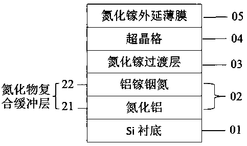
[0023] Such as figure 1 As shown, the present invention provides a method for growing a GaN epitaxial film material without cracks on the surface on a Si substrate, and the structure in the figure is prepared by the following steps:

[0024] Step 1: Select a piece of single crystal Si as the substrate;

[0025] Step 2: epitaxially growing a nitride composite buffer layer on the Si substrate, the nitride composite buffer layer can relieve the lattice mismatch and prevent the remelting etching reaction;

[0026] Step 3: growing a GaN transition layer on the nitride composite buffer layer;

[0027] Step 4: grow a set of superlattice on the GaN transition layer, the superlattice can release part of the tensile stress and filter part of the threading dislocati...


PUM

PropertyMeasurementUnit
thicknessaaaaaaaaaa
thicknessaaaaaaaaaa
thicknessaaaaaaaaaa

Abstract

The invention discloses a method for growing a gallium nitride film on a silicon substrate. According to the method for growing the gallium nitride film on the silicon substrate, a nitride composite buffer layer is epitaxially grown on the Si substrate, and the nitride composite buffer layer can relieve lattice mismatch and prevent a reflow etching reaction. A group of superlattices are grown on aGaN transition layer, and the superlattices can release part of tensile stress and can filter part of threading dislocation. By adopting the method, the crystal quality of a GaN epitaxial film material can be significantly improved, surface cracks are eliminated, and the GaN epitaxial film material which can be used for device development and application is obtained.

Description

technical field [0001] The invention belongs to the technical field of semiconductors, and in particular refers to a gallium nitride (GaN) thin film material with no cracks on the surface grown by heterogeneous epitaxial growth on a silicon (Si) substrate by using a nitride compound buffer layer method. Background technique [0002] As a typical representative of the third-generation wide bandgap semiconductor material, GaN material has outstanding advantages such as large bandgap width, high electron drift speed, high pressure resistance, high temperature resistance, corrosion resistance and radiation resistance, and is especially suitable for the development and production of high temperature and high frequency large Power radio frequency microwave devices and power electronic devices have broad application prospects in the fields of wireless communication, radar, and semiconductor lighting. [0003] However, due to the lack of homogeneous substrates for GaN materials, het...

Claims


Application Information

Patent Timeline
Patent Type & Authority Applications(China)
IPC IPC(8): H01L21/02B82Y40/00
CPCB82Y40/00H01L21/02381H01L21/02458H01L21/02505H01L21/02507H01L21/0254H01L21/0262
Inventor 王晓亮李百泉肖红领
Owner BEIJING HUAJINCHUANGWEI ELECTRONICS CO LTD
Why Eureka
Try Eureka