

SiC power device
A technology of power devices and N-type semiconductors, which is applied to semiconductor devices, electrical components, diodes, etc., can solve the problems of inability to adopt silicon-based conventional reverse conduction structures, slow turn-off speed of SiCIGBT, and large reverse recovery charge, etc., to achieve Elimination of minority carrier injection effect, small electric field reduction effect, and small leakage current effect
- Summary
- Abstract
- Description
- Claims
- Application Information
AI Technical Summary
Problems solved by technology
Method used
Image

Examples
Embodiment 1
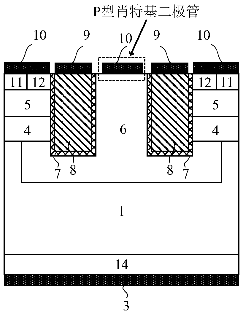
[0062] This embodiment provides a SiC MOSFET device integrating a PN junction body diode, and its cell structure is as follows figure 1 As shown, it includes: an N-type lightly doped region 1 as a withstand voltage region;
[0063]An N-type heavily doped ohmic contact region 14 disposed on the lower surface of the withstand voltage region 1, and an anode metal 3 covering the lower surface of the N-type heavily doped ohmic contact region 14;
[0064] Two separate gate deep grooves arranged on the upper surface of the withstand voltage region 1; the gate deep grooves are composed of an oxide layer 7 on the groove wall and a conductor 8 filled in the groove wall, and the conductor 8 is covered with Gate electrode metal 9; the semiconductor surfaces on the outside of the two gate deep grooves are respectively provided with a P-type semiconductor region base region 5, and the base region 5 is in contact with the groove wall; The contacted N-type heavily doped region 12 as the cat...
Embodiment 2
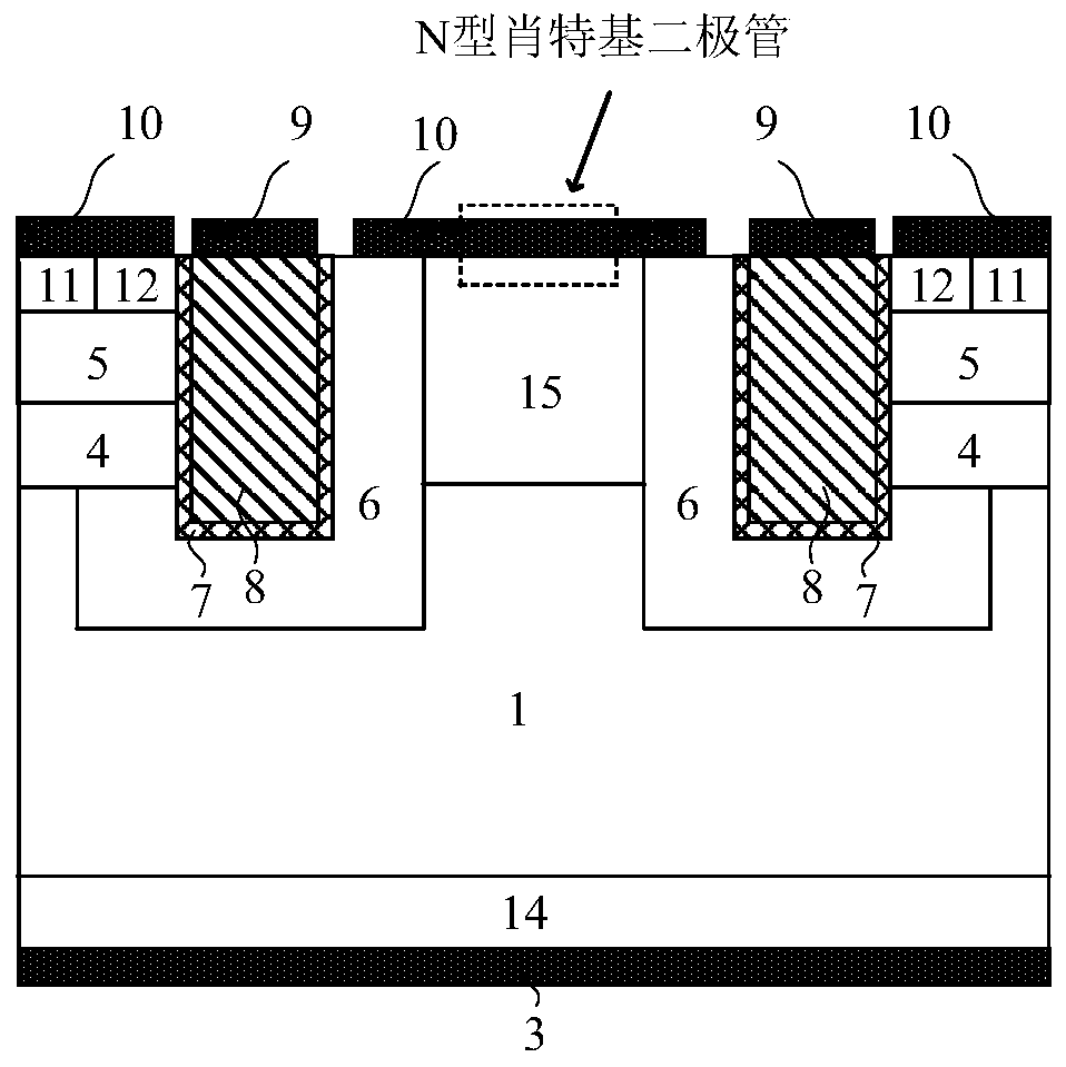
[0069] This embodiment provides a SiC MOSFET device integrating an N-type anti-parallel Schottky diode, and its cell structure is as follows: figure 2 As shown, the difference from Embodiment 1 is that: the P-type semiconductor region 6 is also provided with an N-type semiconductor region 15, and the N-type semiconductor region 15 is located between two gate deep grooves, and the P-type semiconductor region The region 6 is divided into two parts, and the lower surface of the N-type semiconductor region 15 is in contact with the withstand voltage region 1, and the upper surface forms a Schottky contact with the cathode metal 10;
[0070] When the MOSFET conducts in the reverse direction, since the conduction voltage drop of the N-type Schottky diode is lower than that of the PN junction diode, only the N-type Schottky diode participates in conduction, thus avoiding the minority carrier injection effect and reducing the Conduction loss and reverse recovery loss, EMI, etc.
Embodiment 3
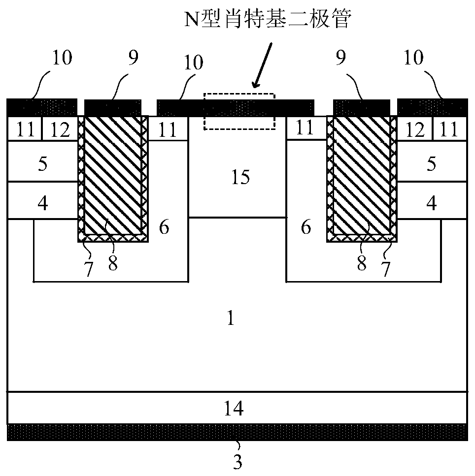
[0072] This embodiment provides a SiC MOSFET device integrating an N-type anti-parallel Schottky diode, and its cell structure is as follows: image 3 As shown, it differs from Embodiment 2 in that the two parts of the P-type semiconductor region 6 located on both sides of the N-type semiconductor region 15 respectively form ohmic contacts with the cathode metal 10 through the P-type heavily doped region 11 at the semiconductor surface.
PUM
 Abstract
Description
Claims
Application Information