
AlGaN/GaN ohmic contact electrode and preparation method and application thereof

A technology of ohmic contact electrodes and electrodes, which is applied in the direction of circuits, electrical components, semiconductor devices, etc., can solve the problems of increased difficulty in multi-layer metal deposition, reduced yield, unfavorable industrialization, etc., to maintain two-dimensional electron gas concentration, low Effect of electrode surface roughness, low ohmic contact value

Inactive Publication Date: 2020-02-14
SOUTH UNIVERSITY OF SCIENCE AND TECHNOLOGY OF CHINA
View PDF4 Cites 5 Cited by
  • Summary
  • Abstract
  • Description
  • Claims
  • Application Information

AI Technical Summary

Problems solved by technology

At present, regarding the gold-free ohmic contact, the minimum ohmic contact value achieved by the recess process is 0.21Ω·mm, which is far from enough for radio frequency devices, and the deposition of multiple metal layers greatly increases the complexity of the process and reduces the process stability
The addition of additional layers of Ta layer or Si layer will further increase the complexity of the film layer, and it is necessary to provide a variety of different metal targets and target positions in the process of preparing the film, which is not conducive to the stability of the coating chamber , the difficulty of multi-layer metal deposition will directly reduce the yield rate, which is not conducive to industrialization

Method used


Image

  • AlGaN/GaN ohmic contact electrode and preparation method and application thereof
  • AlGaN/GaN ohmic contact electrode and preparation method and application thereof
  • AlGaN/GaN ohmic contact electrode and preparation method and application thereof

Examples


Embodiment 1

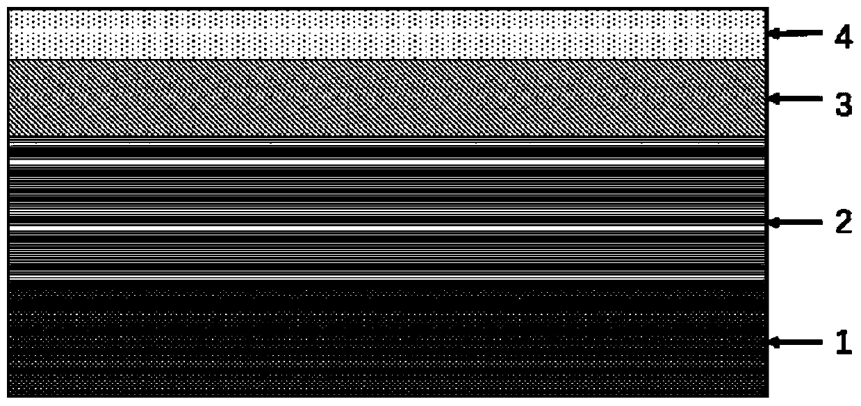
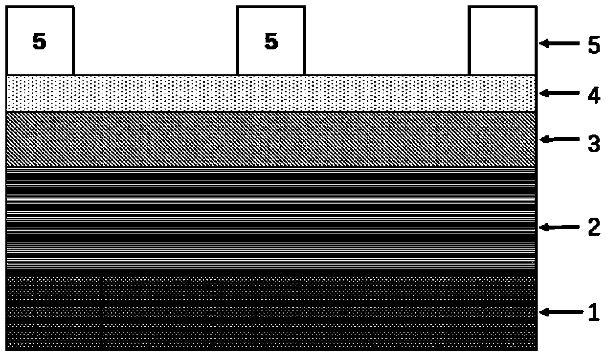
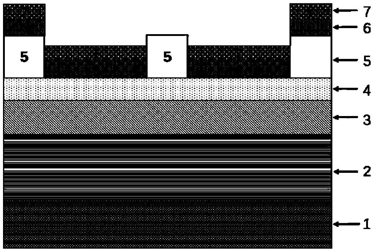
[0060] This embodiment provides a method for preparing an AlGaN / GaN ohmic contact electrode, including the following steps:

[0061] (1) The AlGaN / GaN substrate was ultrasonically cleaned with acetone for 5 minutes, isopropanol for 15 minutes, deionized water for 10 minutes, and dried with nitrogen.

[0062] (2) On the AlGaN layer, perform the process steps of uniform coating, pre-baking, photolithography, development, and post-baking in sequence, define the drain and source patterns, and immerse in HCl:H 2 O=1:4 hydrochloric acid solution for 3 minutes to remove oxides on the surface of the substrate, then rinse with deionized water for 15 minutes, and finally blow dry with nitrogen.

[0063] (3) Immediately put the sample processed in step (2) into the vacuum transfer chamber of the magnetron sputtering equipment to perform the coating process. Ti 10 al 1 The alloy layer is deposited by magnetron sputtering with a thickness of 60nm, and the metal layer of the TiN cap laye...

Embodiment 2

[0066] This embodiment provides a method for preparing an AlGaN / GaN ohmic contact electrode, including the following steps:

[0067] (1) The AlGaN / GaN substrate was ultrasonically cleaned with acetone for 5 minutes, isopropanol for 15 minutes, deionized water for 10 minutes, and dried with nitrogen.

[0068] (2) On the AlGaN layer, perform the process steps of uniform coating, pre-baking, photolithography, development, and post-baking in sequence, define the drain and source patterns, and immerse in HCl:H 2 O=1:4 hydrochloric acid solution for 5 minutes to remove oxides on the surface of the substrate, then rinse with deionized water for 15 minutes, and finally blow dry with nitrogen.

[0069] (3) Immediately put the sample processed in step (2) into the vacuum transfer chamber of the magnetron sputtering equipment to perform the coating process. Ti 5 al 1 The alloy layer is deposited 20nm by magnetron sputtering, and the metal layer of the TiN cap layer is deposited on a T...

Embodiment 3

[0074] This embodiment provides a method for preparing an AlGaN / GaN ohmic contact electrode, including the following steps:

[0075] (1) The AlGaN / GaN substrate was ultrasonically cleaned with acetone for 10 minutes, isopropanol for 5 minutes, deionized water for 15 minutes, and dried with nitrogen.

[0076] (2) On the AlGaN layer, perform the process steps of uniform coating, pre-baking, photolithography, development, and post-baking in sequence, define the drain and source patterns, and immerse in HCl:H 2 O=1:4 hydrochloric acid solution for 2 minutes to remove oxides on the surface of the substrate, then rinse with deionized water for 5 minutes, and finally blow dry with nitrogen.

[0077] (3) Immediately put the sample processed in step (2) into the vacuum transmission chamber of the ion sputtering equipment to perform the coating process. Ti 1 al 1 The alloy layer is deposited by ion sputtering to 40nm, and the metal layer of the TiN cap layer is deposited on a Ti targ...


PUM

PropertyMeasurementUnit
thicknessaaaaaaaaaa
thicknessaaaaaaaaaa

Abstract

The invention relates to an AlGaN / GaN ohmic contact electrode and a preparation method and application thereof. The AlGaN / GaN ohmic contact electrode sequentially comprises an AlGaN / GaN substrate, a cap-layer metal layer and a TixAly alloy layer from bottom to top, wherein x is greater than 0, and y is greater than 0. The preparation method comprises the following steps: defining drain and / or source patterns on an AlGaN layer by using a photoetching technology; sequentially depositing the TixAly alloy and the cap-layer metal layer on the surface of the AlGaN layer; removing a photoresist; performing stripping treatment; and performing heat treatment on a stripped sample to obtain the AlGaN / GaN ohmic contact electrode. The invention further provides a method for reducing ohmic contact between the AlGaN / GaN substrate and an electrode. The method is realized by depositing the TixAly alloy layer on the surface of the AlGaN / GaN substrate for functioning as the electrode. The ohmic contact electrode provided by the invention reaches the preparation standard of a radio frequency device; and meanwhile, the stability and the reliability of the device are improved.

Description

technical field [0001] The invention relates to the technical field of electronic semiconductor devices, in particular to an AlGaN / GaN ohmic contact electrode and its preparation method and application. Background technique [0002] The third-generation semiconductor material gallium nitride (GaN) has a wide band gap, high breakdown electric field, high thermal conductivity, high electron saturation rate and higher radiation resistance. There are broad application prospects in semiconductor devices. Among them, AlGaN / GaN HEMTs (AlGaN / GaN High Electron Mobility Transistors) have two-dimensional electron gas (2DEG) with high electron mobility, and have great application prospects in radio frequency and power switching devices. [0003] The ohmic contact quality of AlGaN / GaN HEMTs devices is an important indicator that affects the final output parameters of the device, and directly affects the source-drain output current, on-resistance, and breakdown voltage of the device. Hi...

Claims


Application Information

Patent Timeline
Patent Type & Authority Applications(China)
IPC IPC(8): H01L29/40H01L29/45H01L29/778
CPCH01L29/40H01L29/401H01L29/45H01L29/452H01L29/778
Inventor 于洪宇蒋玉龙范梦雅
Owner SOUTH UNIVERSITY OF SCIENCE AND TECHNOLOGY OF CHINA
Learn More