Structure for realizing medium-/high-frequency alternating-current driving of OLED by using TADF
A high-frequency AC and AC drive technology, applied in the manufacturing of electrical components, electro-solid devices, semiconductor/solid-state devices, etc., can solve the problems of process complexity and complex DC drive integration, achieve simple and controllable processes, and improve quantum efficiency. , promote the effect of injection
- Summary
- Abstract
- Description
- Claims
- Application Information
AI Technical Summary
Problems solved by technology
Method used
Image
Examples
preparation example Construction
[0051] The structure of using TADF to realize medium and high frequency AC driven OLED, its preparation method comprises the following steps;
[0052] Step B1, using the anode layer substrate as the anode electrode layer;
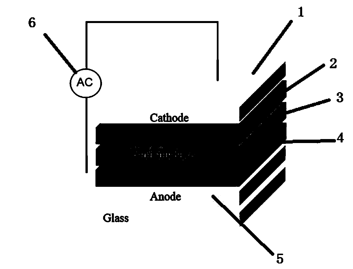
[0053] Step B2, forming a first piezoelectric functional layer on the anode electrode layer by a deposition process; then forming a light-emitting layer on the first piezoelectric functional layer by a deposition process; and then forming a second piezoelectric functional layer on the light-emitting layer by a deposition process ; Finally, a cathode electrode layer is formed on the second piezoelectric functional layer by a deposition process.
[0054] Both the piezoelectric functional layer and the luminescent layer are formed by a solution method or a vacuum evaporation method; the solution method includes spin coating, dip coating, blade coating, spray coating, screen printing, slit coating or spray coating. ink printing.
[0055] The frequency range o...
Embodiment 1
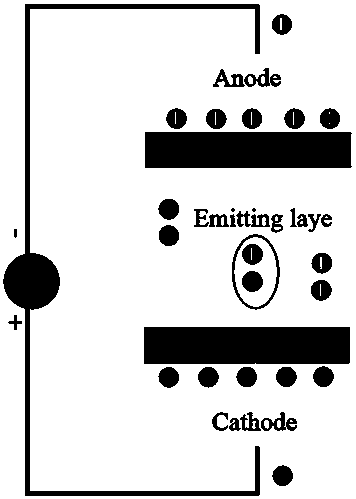
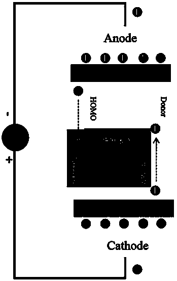
[0059] In this example, the structure of using TADF to realize medium and high frequency AC driving OLED is an OLED device with a laminated structure, including a conductive anode (anode electrode layer) deposited sequentially on the light-emitting surface, and two piezoelectric functional layers (the first Piezoelectric functional layer, the second piezoelectric functional layer) and a sandwich structure composed of a light-emitting layer in between, a conductive cathode (cathode electrode layer); two electrode layers form two transparent electrodes; applied between the two transparent electrodes AC drive signal; the light emitting surface adopts glass substrate.
Embodiment 2
[0061] In Embodiment 1, the material of the first piezoelectric functional layer and the second piezoelectric functional layer is silicic acid, which has a high dielectric constant and is a transparent material, which can be used as a preferred inorganic insulating functional layer material.
[0062] The thickness of the piezoelectric functional layer is 5-50nm. In this thickness range, the insulating effect is better, and the response speed of the organic light-emitting device can be accelerated, and at the same time, the organic light-emitting device can be packaged, that is, the organic light-emitting device can be packaged. Light-emitting devices have a good protective effect. If it is lower than this range, the insulating dielectric layer cannot encapsulate the organic light-emitting device; if it is higher than this range, although it can protect the organic light-emitting device, it reduces the response speed of the OLED device and reduces the actual effect of the produ...
PUM
| Property | Measurement | Unit |
|---|---|---|
| thickness | aaaaa | aaaaa |
| thickness | aaaaa | aaaaa |
| thickness | aaaaa | aaaaa |
Abstract
Description
Claims
Application Information


