Protective layer for semiconductor thin film transistor and its realization and application method

A thin-film transistor and semiconductor technology, applied in the manufacture of transistors, semiconductor devices, semiconductor/solid-state devices, etc., can solve problems such as unstable illumination, achieve stable and reliable illumination stability, good shading effect, and suppress the change of defect states. Effect

Active Publication Date: 2021-01-08
SHANGHAI JIAOTONG UNIV
View PDF3 Cites 0 Cited by
  • Summary
  • Abstract
  • Description
  • Claims
  • Application Information

AI Technical Summary

Problems solved by technology

[0004] Aiming at the light instability problem of the existing amorphous oxide semiconductor thin film transistors, the present invention proposes a protective layer for semiconductor thin film transistors and its realization and application method. layer and nitrogen-doped process (channel layer) to obtain an amorphous oxide semiconductor thin film transistor with high light stability

Method used


Image

  • Protective layer for semiconductor thin film transistor and its realization and application method
  • Protective layer for semiconductor thin film transistor and its realization and application method
  • Protective layer for semiconductor thin film transistor and its realization and application method

Examples


Embodiment 1

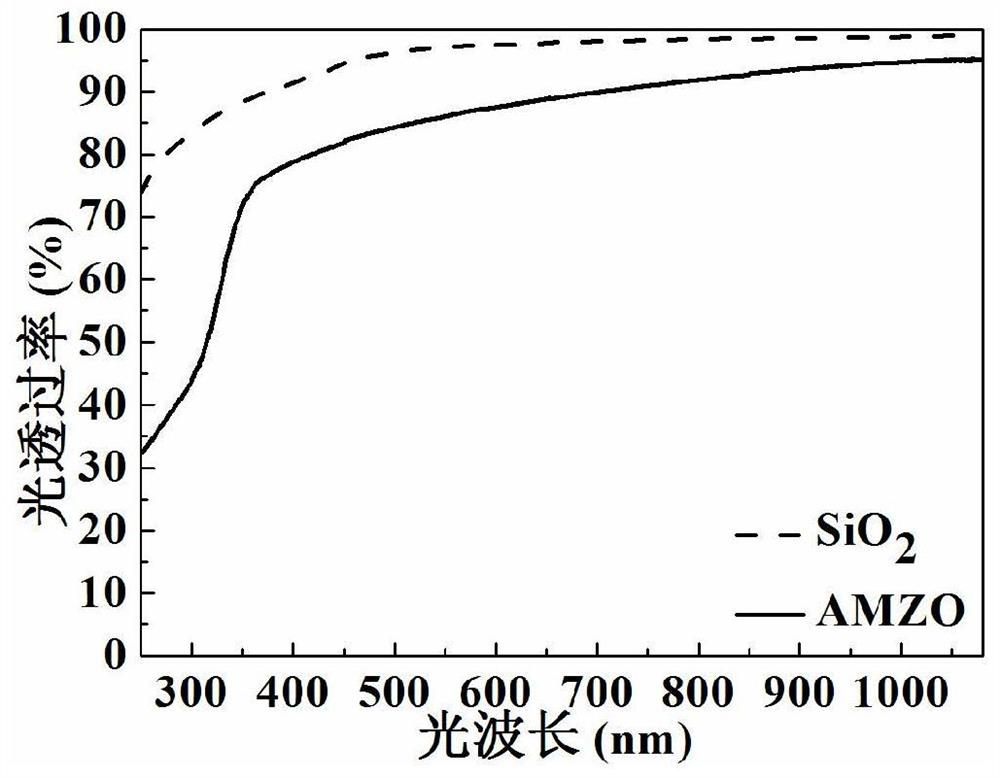
[0034] Such as figure 1 As shown, it is a kind of Al-Mn-Zn oxide thin film with better shielding short-wavelength UV light and traditional SiO 2 Schematic diagram of the comparison of light transmittance of the film, in which the aluminum manganese zinc oxide film is Al 2 o 3 , MnO and ZnO three dopants are mixed and ground, pressed into a target, sintered to obtain an Al-Mn-Zn oxide target, and then sputtered by a magnetron sputtering device.

[0035] The three components described (Al 2 o 3 , MnO and ZnO), the doping amount of each component ranges from 3% to 90%wt%. In this embodiment, the target ratio used is Al 2 o 3 :MnO:ZnO=6:5:89wt%.

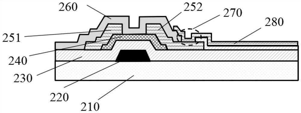
[0036] Such as figure 2 As shown, it is a nitrogen-doped amorphous oxide semiconductor thin film transistor using a single-layer aluminum-manganese-zinc oxide thin film as a protective layer in this embodiment, including: a gate electrode layer 220 sequentially formed on a glass substrate 210 , a gate insulating layer 230 , a ni...

Embodiment 2

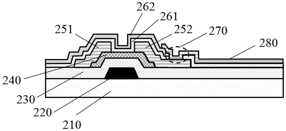
[0043] Such as image 3 As shown, it is a kind of double-layer Al-Mn-Zn oxide / SiO 2 A nitrogen-doped amorphous oxide semiconductor thin film transistor with a thin film as a protective layer. Compared with Embodiment 1, the protective layer in this embodiment includes: a first protective layer 261 and a second protective layer 262, wherein: the first protective layer 261 It is located on the active layer 240 , the drain electrode layer 251 and the source electrode layer 252 and is located under the second protection layer 262 .

[0044] The first protective layer 261 is SiO 2 The thin film is prepared by magnetron sputtering or PECVD equipment, and its thickness is 50nm;

[0045] The second protection layer 262 is an Al-Mn-Zn oxide thin film prepared by magnetron sputtering with a thickness of 50 nm.

[0046] Such as Figure 5 As shown, it is a schematic flow chart of the preparation process of the nitrogen-doped amorphous oxide semiconductor thin film transistor based on ...


PUM

PropertyMeasurementUnit
thicknessaaaaaaaaaa
thicknessaaaaaaaaaa

Abstract

The invention relates to a protective layer for a semiconductor thin film transistor and an implementation and application method thereof. The protective layer for a semiconductor thin film transistoris actually an aluminum-manganese-zinc oxide (AMZO) thin film, which consists of aluminum oxide Al2O3, manganese oxide MnO and zinc oxide ZnO with the doping amount ranges of 3% to 90%wt%. A single-layer AMZO thin film or a double-layer SiO2 / AMZO thin film is deposited on a thin film transistor through magnetron sputtering to serve as a device protective layer. The single-layer AMZO protective layer can shield ultraviolet light with short wavelength and transmit visible light with relatively long wavelength, so that the illumination stability of the nitrogen-doped amorphous oxide semiconductor thin film transistor is greatly improved. The double-layer SiO2 / AMZO protective layer solves the problem of degradation of device operation characteristics caused by the single-layer AMZO protectivelayer, and meanwhile, the nitrogen-doped amorphous oxide semiconductor thin film transistor with high stability can be obtained.

Description

technical field [0001] The invention relates to a technology in the semiconductor field, in particular to a protective layer for a nitrogen-doped amorphous oxide semiconductor thin film transistor and its realization and application method. Background technique [0002] Amorphous oxide semiconductor thin film transistors (typically represented by amorphous indium gallium zinc oxide thin film transistors (a-IGZO TFTs)) have high mobility (μ FE >10cm 2 / V·s), high switching current ratio (I ON / I OFF >10 8 ), high visible light transmittance (>80%) and low temperature process technology (room temperature magnetron sputtering) and many other advantages, but its electrical characteristics are easily affected by light (especially short-wavelength UV light) and ambient atmosphere (such as oxygen, water vapor), etc., showing unstable electrical characteristics. [0003] In order to reduce the impact of environmental factors on amorphous oxide semiconductor thin film t...

Claims


Application Information

Patent Timeline
Patent Type & Authority Patents(China)
IPC IPC(8): H01L29/786H01L21/473H01L21/34
CPCH01L21/02172H01L21/02266H01L29/66969H01L29/78633H01L29/78693
Inventor 解海艇董承远
Owner SHANGHAI JIAOTONG UNIV
Why Eureka
Try Eureka