Check patentability & draft patents in minutes with Patsnap Eureka AI!

A semiconductor device with trench gate and manufacturing method thereof

A trench gate, manufacturing method technology, applied in semiconductor/solid-state device manufacturing, semiconductor devices, electrical components and other directions, can solve the problems of difficult process, impurity diffusion, affecting the performance of IGBT transistor devices, etc., to improve performance, Enhanced adhesion, reduced lateral size

Active Publication Date: 2020-03-24
SEMICON MFG ELECTRONICS (SHAOXING) CORP
View PDF6 Cites 4 Cited by
  • Summary
  • Abstract
  • Description
  • Claims
  • Application Information

AI Technical Summary

Problems solved by technology

However, as the size of semiconductor devices becomes smaller and the technical specifications become higher and higher, the critical dimension (CDsize) reserved for the small-sized IGBT transistor device structure from the contact hole to the gate trench on the design side gradually becomes smaller. When using wet etching to form contact holes, there are the following problems that affect the performance of the fabricated IGBT transistor device: 1) the process is difficult due to the reduction of critical dimensions; 2) wet etching is isotropic , when wet etching reaches the required depth of the contact hole, the accompanying lateral etching will often be too much, which will cause the distance between the contact hole formed after wet etching and the gate trench to be too small, which will lead to subsequent contact holes. Impurities implanted in the hole will diffuse to the channel region after annealing, thereby increasing the threshold voltage of the IGBT transistor device

Method used


Image

  • A semiconductor device with trench gate and manufacturing method thereof
  • A semiconductor device with trench gate and manufacturing method thereof
  • A semiconductor device with trench gate and manufacturing method thereof

Examples


Embodiment Construction

[0034] The technical solutions proposed by the present invention will be described in further detail below in conjunction with the accompanying drawings and specific embodiments. It should be noted that all the drawings are in a very simplified form and use imprecise scales, and are only used to facilitate and clearly assist the purpose of illustrating the embodiments of the present invention.

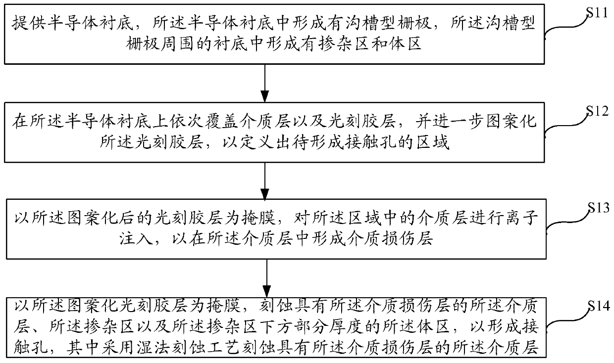
[0035] Please refer to figure 1 , an embodiment of the present invention provides a method for manufacturing a semiconductor device with a trench gate, including:

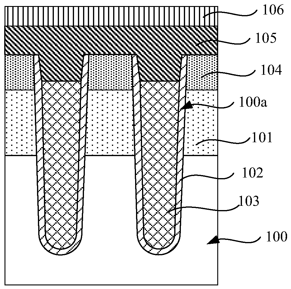
[0036] S11, providing a semiconductor substrate, a trench gate is formed in the semiconductor substrate, and a doped region and a body region are formed in the substrate around the trench gate;

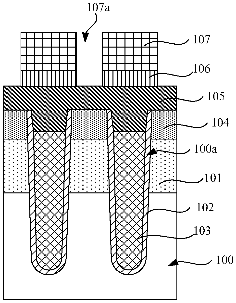
[0037] S12, sequentially covering a dielectric layer and a photoresist layer on the semiconductor substrate, and further patterning the photoresist layer to define a region where a contact hole is to be formed;

[0038] S13, usin...


PUM


Abstract

The invention provides a semiconductor device with a trench gate and a manufacturing method thereof. The method comprises the following steps: after a patterned photoresist layer is formed, performingion implantation on a dielectric layer with partial thickness or total thickness; forming a dielectric damage layer in the dielectric layer, carrying out wet etching on the dielectric layer with thedielectric damage layer and further carrying out wet etching or dry etching on the doped region below and the body region with partial thickness to form contact hole. In the process of wet etching ofa dielectric layer with a dielectric damage layer, the dielectric damage layer and the dielectric layer around the dielectric damage layer have a high etching selection ratio. Therefore, the process difficulty can be reduced, the transverse etching can be reduced, the morphology of the finally manufactured contact hole can be improved, the distance between the bottom of the formed contact hole andthe trench type gate can be ensured, and the performance of the finally manufactured trench type semiconductor device can be improved.

Description

technical field [0001] The invention relates to the technical field of semiconductor manufacturing, in particular to a semiconductor device with a trench gate and a manufacturing method thereof. Background technique [0002] At present, the technology of IGBT (Insulated Gate Bipolar Transistor, insulated gate bipolar transistor) and VDMOS (Vertical Double-diffused MOSFET, vertical channel double-diffused metal oxide transistor) is constantly innovating, and the size of power semiconductor devices is constantly being realized. Under the premise of shrinking, the excellent performance of power semiconductor devices is also guaranteed. [0003] In the manufacturing process of the existing trench type IGBT transistor, it is necessary to transfer the design pattern of the contact hole from the mask plate to the wafer (i.e., the substrate) by means of a photolithography process and an etching process after the trench type gate is completed. ), specifically, a patterned photoresis...

Claims


Application Information

Patent Timeline
IPC IPC(8): H01L21/331H01L21/336H01L29/739H01L29/78H01L21/768
CPCH01L29/66325H01L29/66734H01L29/7393H01L29/7813H01L21/76802H01L21/76825
Inventor 帅露王珏余龙
Owner SEMICON MFG ELECTRONICS (SHAOXING) CORP
Features
  • R&D
  • Intellectual Property
  • Life Sciences
  • Materials
  • Tech Scout
  • Unparalleled Data Quality
  • Higher Quality Content
  • 60% Fewer Hallucinations
Learn More