Supercharge Your Innovation With Domain-Expert AI Agents!

SOI pressure sensor piezoresistor, manufacturing method thereof and SOI pressure sensor

A technology of pressure sensor and piezoresistor, which is applied in the manufacture/assembly of piezoelectric/electrostrictive devices, semiconductor/solid-state device manufacturing, piezoelectric/electrostrictive/magnetostrictive devices, etc., which can solve surface roughness, The stress cannot be effectively transmitted, and the uniformity of the ion beam cannot be guaranteed.

Active Publication Date: 2020-03-24
48TH RES INST OF CHINA ELECTRONICS TECH GROUP CORP
View PDF7 Cites 3 Cited by
  • Summary
  • Abstract
  • Description
  • Claims
  • Application Information

AI Technical Summary

Problems solved by technology

However, the existing etching equipment and etching process still have the following problems: (1) the etching equipment used in the existing MEMS is expensive, and the cost of improving the etching equipment is high; (2) the existing piezoresistive etching mainly uses Dry etching. In dry etching, the silicon in the area without photoresist protection is removed by means of ion beam bombardment, thereby forming piezoresistive. However, in the dry etching process, there is usually a certain curvature between the etched side and the bottom corner. The bottom and sides of the etched area are rough in a small area due to ion bombardment. From a microscopic point of view, the piezoresistive surface formed by ion beam etching has a local small island structure, and the local small island has a stress concentration phenomenon. The stress distribution is uneven, which makes the measurement accuracy of the sensor lower; further, in the dry etching process, the etching selection ratio between different media is usually small, such as the selection ratio of silicon and silicon dioxide is usually less than 5:1, in order to ensure that the top silicon film is etched clean, a certain amount of over-etching is usually required, and the silicon dioxide layer below will continue to be etched after the silicon etching in the faster-etched area during the over-etching process (BOX layer), as a result, the BOX layer is also etched to a certain thickness, and the increase in the distance between the piezoresistive and the strain diaphragm surface will lead to relaxation of the piezoresistive stress, so that the stress cannot be effectively transmitted to the piezoresistor, reducing the sensitivity of the sensor, resulting in The measurement accuracy of the sensor is reduced; in addition, when the photoresist is usually used as the etching barrier layer in the dry etching process, the photoresist is directly in contact with the silicon piezoresistive surface, and it is easy to introduce organic contamination, and these organic contamination The existence of is not conducive to the accurate measurement of stress by SOI pressure sensor
The existence of the above problems makes it difficult for existing SOI pressure sensors to meet the needs of aerospace and other fields for high temperature resistance and high precision.
In addition, with the development of technology, the size of silicon wafers corresponding to MEMS technology is also getting larger and larger. In the whole area of ​​larger silicon wafers, there are still certain technical challenges in ensuring good uniformity of ion beams. The uniformity of the beam cannot ensure the uniformity of the etching of the entire silicon wafer, so that the yield of the product cannot be guaranteed
In addition, the etching equipment used in the existing MEMS is expensive, and the cost of improving the process by improving the etching equipment is even higher

Method used


Image

  • SOI pressure sensor piezoresistor, manufacturing method thereof and SOI pressure sensor
  • SOI pressure sensor piezoresistor, manufacturing method thereof and SOI pressure sensor
  • SOI pressure sensor piezoresistor, manufacturing method thereof and SOI pressure sensor

Examples


Embodiment 1

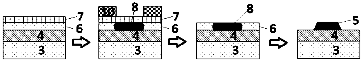
[0048] A kind of manufacturing method of SOI pressure sensor piezoresistor, its manufacturing process flow chart is as follows figure 1 shown, including the following steps:

[0049] (1) Prepare a buffer protection layer 7 on the surface of the top silicon 6 of the SOI sheet, specifically: grow a silicon dioxide film on the surface of the top silicon by thermal oxidation, with a thickness of 80 Å.

[0050] (2) The surface of the buffer protection layer 7 obtained in step (1) is subjected to uniform photolithography and development to prepare an injection barrier layer 10, exposing areas such as piezoresistors and interconnection pads, and using ion implantation to compress the top layer of silicon. P-type doping is performed on areas such as sensitive resistors and interconnection pads to form a P-type heavily doped region 8, wherein the average doping concentration in the P-type heavily doped region 8 is 2×10 20 cm -3 ; The non-P-type heavily doped region is N-type or P-typ...

Embodiment 2

[0056] A kind of manufacturing method of SOI pressure sensor piezoresistor, its manufacturing process flow chart is as follows Figure 4 shown, including the following steps:

[0057] (1) Prepare a buffer protection layer 7 on the surface of the top silicon 6 of the P-type SOI sheet, specifically: grow a silicon dioxide film on the surface of the top silicon by thermal oxidation, with a thickness of 100 Å.

[0058] (2) Perform P-type doping on the top layer of silicon prepared with buffer protection layer 7 on the surface in step (1) by diffusion doping, and anneal to form P-type heavily doped region 8 . In this step, when the difference in doping concentration between the P-type non-doped region and the P-type heavily doped region is small, for example, the doping concentration of the non-P-type heavily doped region is 1×10 18 cm -3 , P-type heavily doped region concentration 3×10 18 cm -3 When , or when the entire top silicon layer is heavily doped with P type, the diffe...

Embodiment 3

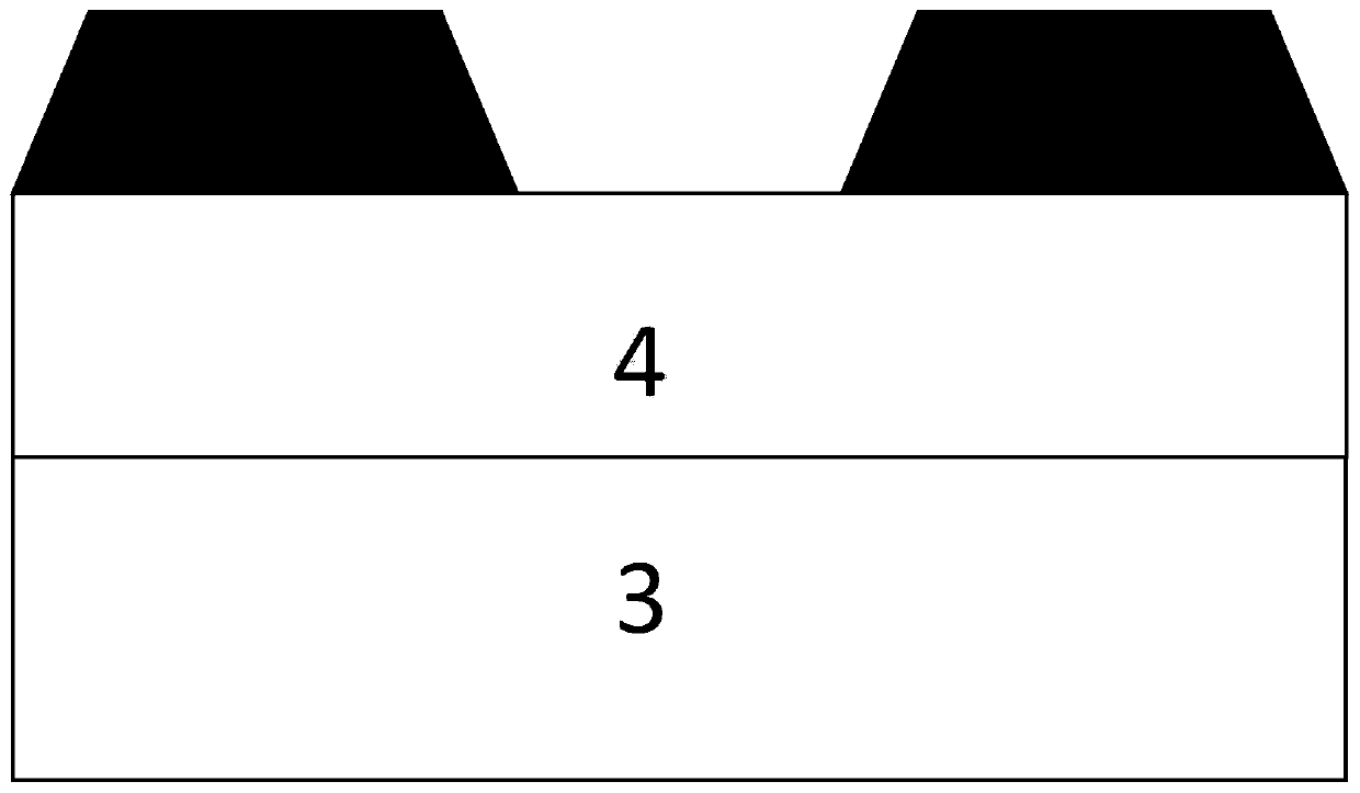
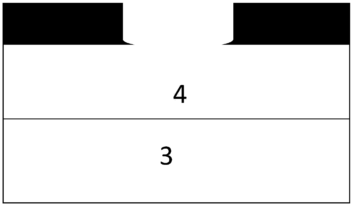
[0066] An SOI pressure sensor such as Figure 5 As shown, it includes a substrate sheet 1 and a functional chip 3, a BOX layer 4, and a P-type heavily doped piezoresistor 5 arranged sequentially on the substrate sheet from bottom to top, wherein a stress reference cavity 2 is also included between the substrate sheet and the functional chip. , P-type heavily doped piezoresistor 5 is the SOI pressure sensor piezoresistor prepared in Example 1.

[0067] In this embodiment, the substrate chip 1 is a bonded silicon chip; the functional chip 3 is an N-type silicon chip, and the doping concentration is less than 1×10 18 cm -3 ; The stress reference cavity 2 is a stress reference cavity of a vacuum pressure sensor, and its cavity structure is a C-shaped strain cavity structure.


PUM

PropertyMeasurementUnit
Thicknessaaaaaaaaaa
Doping concentrationaaaaaaaaaa
Thicknessaaaaaaaaaa

Abstract

The invention discloses an SOI pressure sensor piezoresistor and a manufacturing method thereof, and an SOI pressure sensor. The manufacturing method comprises the following steps: preparing an injection buffer protection layer, and preparing an injection barrier layer; performing P-type doping and annealing to form a P-type heavily doped region; and removing the non-P-type heavily doped region bywet etching to obtain the piezoresistor of the SOI pressure sensor. The piezoresistor of the SOI pressure sensor is prepared by the method. The SOI pressure sensor comprises a P-type heavily doped piezoresistor, and the P-type heavily doped piezoresistor is the piezoresistor of the SOI pressure sensor. The manufacturing method of the SOI pressure sensor piezoresistor has the advantages of being low in cost, high in etching precision, good in consistency, high in mass production efficiency, little in secondary pollution and the like, the surface of the manufactured piezoresistor is straight and smooth, and the piezoresistor can be widely used as a piezoresistor of an SOI pressure sensor and has high use value and good application prospects.

Description

technical field [0001] The invention belongs to the technical field of pressure sensor preparation, and relates to an SOI pressure sensor piezoresistor, a manufacturing method thereof, and an SOI pressure sensor. Background technique [0002] With the continuous development of aviation, aerospace, petrochemical and other fields, the demand for pressure sensors in these fields is increasing, and the demand for pressure measurement under special environmental conditions is also increasingly urgent. Therefore, pressure sensors such as: High temperature, high precision, high reliability, miniaturization and other requirements. [0003] Traditional bulk silicon pressure sensors use ordinary N-type bulk silicon wafers. Silicon piezoresistors are obtained by performing P-type doping in the piezoresistive and interconnection areas. The piezoresistive and substrate are separated by a PN junction without a separate silicon pressure sensor. Resistance to etching, but as the working te...

Claims


Application Information

Patent Timeline
IPC IPC(8): H01L41/113H01L41/22H01L41/27H01L21/306
CPCH01L21/30608H10N30/302H10N30/01H10N30/05
Inventor 曾庆平金忠张浩何峰周国方丁玎吴迪
Owner 48TH RES INST OF CHINA ELECTRONICS TECH GROUP CORP
Features
  • R&D
  • Intellectual Property
  • Life Sciences
  • Materials
  • Tech Scout
  • Unparalleled Data Quality
  • Higher Quality Content
  • 60% Fewer Hallucinations
Learn More