Perovskite/crystalline silicon laminated solar cell and preparation method thereof

A technology of solar cells and perovskite cells, which is applied in the field of solar cells, can solve problems such as the inability to prepare thin layers and the inability to prepare high-efficiency crystalline silicon/perovskite composite cells, and achieve excellent layered structures, improved efficiency, and light conversion high efficiency effect

Pending Publication Date: 2020-04-07
紫石能源有限公司
View PDF0 Cites 8 Cited by
  • Summary
  • Abstract
  • Description
  • Claims
  • Application Information

AI Technical Summary

Problems solved by technology

However, due to the unevenness formed on the surface of the textured structure, it is easy to accumulate in the recesses of the surface during the process of continuing to deposit the hole transport layer of

Method used


Image

  • Perovskite/crystalline silicon laminated solar cell and preparation method thereof
  • Perovskite/crystalline silicon laminated solar cell and preparation method thereof

Examples


Embodiment 1

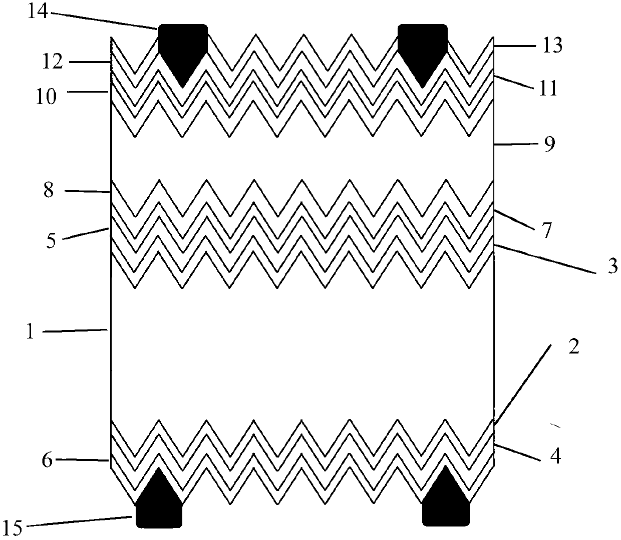
[0118] This embodiment relates to a perovskite / crystalline silicon laminated solar cell, and its specific structure is shown in figure 1 :

[0119] Including a crystalline silicon cell, a composite junction and a perovskite cell, the composite junction 7 is arranged between the crystalline silicon cell and the perovskite cell;

[0120] The crystalline silicon battery includes a crystalline silicon substrate 1, transparent conductive films a 6, p + poly-Si layer 4, the first tunneling layer SiO x 2. The second tunneling layer SiO x 3, and the n + poly-Si layer 5;

[0121] The first tunneling layer SiO x disposed on the first surface of the crystalline silicon substrate, the second tunneling layer SiO x It is arranged on the second surface of the crystalline silicon substrate, the first surface and the second surface of the crystalline silicon substrate are oppositely arranged, and the p + poly-Si layer is provided on the first tunneling layer SiO x away from the side ...

Embodiment 2

[0137] This embodiment relates to a perovskite / crystalline silicon laminated solar cell, which has the same layered structure as that of Embodiment 1, and the only difference lies in the specific selection and thickness of the materials of each layer, specifically:

[0138] The material of described transparent conductive film a is ITO, and the thickness of described transparent conductive film a is 180nm, p + The thickness of the poly-Si layer is 100nm, the first and second tunneling layer SiO x The thickness of the crystalline silicon substrate is 1.5nm, the thickness of the crystalline silicon substrate is 260 microns, n + The poly-Si layer has a thickness of 100 nm.

[0139] The hole transport layer is PEDOT-PSS, and its thickness is 400nm;

[0140] The material of the perovskite layer is MAPbI 3 , and its thickness is 450nm.

[0141] The material of the electron transport layer is PCBM, and its thickness is 100nm;

[0142] The material of the buffer layer is TiO 2 ,...

Embodiment 3

[0147] This embodiment relates to a perovskite / crystalline silicon laminated solar cell, which has the same layered structure as that of Embodiment 1, and the only difference lies in the specific selection and thickness of the materials of each layer, specifically:

[0148] The material of described transparent conductive film a is ITO, and the thickness of described transparent conductive film a is 180nm, p + The thickness of the poly-Si layer is 200nm, the first and second tunneling layer SiO x The thickness of the silicon substrate is 1.8nm, the thickness of the crystalline silicon substrate is 280nm, n + The poly-Si layer has a thickness of 200 nm.

[0149] The hole transport layer is NiO with a thickness of 200nm;

[0150] The material of the perovskite layer is MAPbBr 3 , and its thickness is 400nm.

[0151] The material of the electron transport layer is PCBM, and its thickness is 100nm;

[0152] The material of the buffer layer is Al-doped ZnO, and its thickness i...


PUM

PropertyMeasurementUnit
Thicknessaaaaaaaaaa
Thicknessaaaaaaaaaa
Thicknessaaaaaaaaaa

Abstract

The invention relates to a perovskite/crystalline silicon laminated solar cell. The perovskite/crystalline silicon laminated solar cell comprises a crystalline silicon cell, a composite junction and aperovskite cell, the composite junction is arranged between the crystalline silicon cell and the perovskite cell, the crystalline silicon cell comprises a crystalline silicon substrate, the surface,close to the composite junction, of the crystalline silicon substrate is a textured surface, and the composite junction is made of nc-Si:H(p+)/nc-Si:H (n+). The laminated solar cell is of a suede structure, light reflection can be effectively reduced, the spectral absorption efficiency and the current density are increased, and therefore the photoelectric conversion efficiency is improved. The adopted material is an nc-Si:H (p+)/nc-Si:H (n+) composite junction, deposition of the perovskite cell in a textured structure can be avoided, a uniform thin layer is prepared, and the spectral absorption efficiency and the current density are increased, so that the photoelectric conversion efficiency is improved.

Description

technical field [0001] The invention relates to the field of solar cells, in particular to a perovskite / crystalline silicon stacked solar cell and a preparation method thereof. Background technique [0002] Crystalline silicon solar cell technology is currently the most mature commercial photovoltaic power generation technology, and its theoretical limit efficiency is around 29%. It is difficult to greatly increase the efficiency of crystalline silicon cells. [0003] Finding new materials with excellent optical and electrical properties and silicon to form a heterojunction cell with upper and lower double absorption layers is of great significance for improving the spectral absorptivity and thus the efficiency of solar cells. [0004] Organic / inorganic hybrid perovskites (such as CH 3 NH 3 PB 3 ) material is a research hotspot in the field of solar cells in recent years. Perovskite cells have the advantages of continuously adjustable band gap, high light absorption coef...

Claims


Application Information

Patent Timeline
IPC IPC(8): H01L51/42H01L51/48
CPCH10K30/00Y02E10/549Y02P70/50
Inventor 许吉林
Owner 紫石能源有限公司
Why Eureka
Try Eureka