Microwave power amplifier chip carrier and preparation method thereof
A power amplifier chip and carrier technology, which is applied in the direction of semiconductor devices, electric solid devices, semiconductor/solid device components, etc., can solve the problems of increasing the manufacturing process steps of T/R components, polluting microwave power chips, etc., to meet the requirements of high-efficiency heat dissipation and Low thermal stress requirements, reduced manufacturing processes, and improved reliability
- Summary
- Abstract
- Description
- Claims
- Application Information
AI Technical Summary
Problems solved by technology
Method used
Image
Examples
Embodiment 1
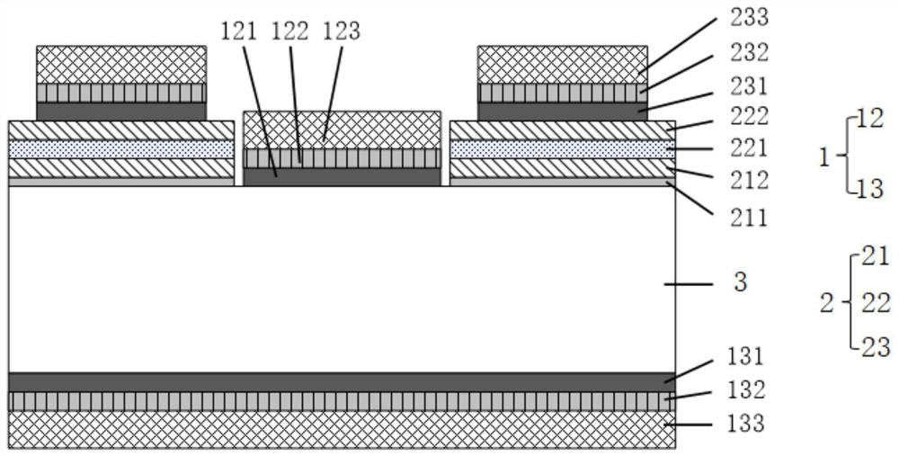
[0044] see figure 1 The microwave power amplifier chip carrier of this embodiment includes: a high-silicon aluminum alloy substrate 3, a chip spacer 1, and a film capacitor 2. The high-silicon aluminum alloy substrate 3 has two parallel planes, which are respectively the first surface and the second surface , the silicon content of the high-silicon aluminum alloy substrate 3 is preferably more than 25%, and its first surface roughness is less than 100 nm, and its second surface roughness is less than 1 μm;
[0045] The chip pad 1 includes a chip bonding metal layer 12 and a carrier bonding metal layer 13. The chip bonding metal layer 12 is formed on the power chip bonding area on the first surface of the high-silicon aluminum alloy substrate 3, and the carrier bonding metal layer 13 is formed on the high-silicon aluminum alloy substrate 3. The second surface of the substrate 3; the die bonding metal layer 12 includes a second metal seed layer 121, a second barrier layer 122 an...
Embodiment 2
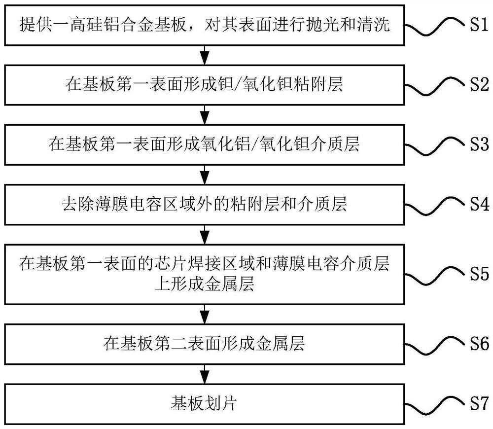
[0052] refer to Figure 2-Figure 9 , this embodiment provides a method for preparing the microwave power amplifier chip carrier provided by Embodiment 1. This embodiment is based on the selection of the same metal for the wire bonding layer 233 and the first soldering layer 123. The specific steps of the method are as follows :
[0053] S1: see image 3 , performing chemical mechanical polishing and cleaning on the first surface and the second surface of the high-silicon aluminum alloy substrate 3, so that the roughness of the first surface is lower than 100 nm, the roughness of the second surface is lower than 1 μm, and the first surface and the second surface are two surfaces of the high-silicon aluminum alloy substrate 3 parallel to each other;
[0054] S2: see Figure 4 , using magnetron sputtering technology, sequentially sputtering tantalum film 211 and tantalum oxide film 212 on the first surface of the high-silicon aluminum alloy aluminum substrate to form an adhesi...
Embodiment 3
[0062] The difference from Example 2 is that in steps S2 to S4, the adhesive layer 21 and the dielectric layer 22 of the thin film capacitor 2 are prepared by using the lift-off process, specifically, glue is first applied on the first surface and the thin film capacitor 2 is pre-embedded by photolithography. For the window, the thin film capacitor 2 is deposited on the first surface of the window pattern on which the thin film capacitor 2 is pre-buried, and then the film in the non-film capacitor 2 area is peeled off by glue removal.
PUM
| Property | Measurement | Unit |
|---|---|---|
| surface roughness | aaaaa | aaaaa |
| surface roughness | aaaaa | aaaaa |
Abstract
Description
Claims
Application Information


