Inorganic-organic hybrid superlattice material with photochromic property as well as preparation and application of inorganic-organic hybrid superlattice material
A technology of organic hybridization and inorganic materials, applied in photovoltaic power generation, semiconductor/solid-state device manufacturing, electrical components, etc., can solve the problems of poor reproducibility and low yield of superlattice, and achieve the effect of simple and easy preparation
- Summary
- Abstract
- Description
- Claims
- Application Information
AI Technical Summary
Problems solved by technology
Method used
Image
Examples
preparation example Construction
[0045] The preparation method of the present invention will be further described in detail in conjunction with specific examples below. It should be understood that the following examples are only for illustrating and explaining the present invention, and should not be construed as limiting the protection scope of the present invention. All technologies realized based on the above contents of the present invention are covered within the scope of protection intended by the present invention.
[0046] The experimental methods used in the following examples are conventional methods unless otherwise specified; the reagents and materials used in the following examples can be obtained from commercial sources unless otherwise specified.
Embodiment 1
[0048] 0.020g PbI 2 and 0.0033g EtDAB were dissolved in 1mLDMF (N,N'-dimethylformamide) to obtain a light yellow clear solution, and 10mL acetonitrile and 30mL chlorobenzene were added to the above clear solution as an antisolvent to obtain a yellow precipitate. The reaction mixture was irradiated under an incandescent lamp, and about 0.021 g of a dark green product was obtained, which was recorded as EtDAB·4PbI 2 , where 4 represents EtDAB and PbI 2 The molar ratio is 1:4.
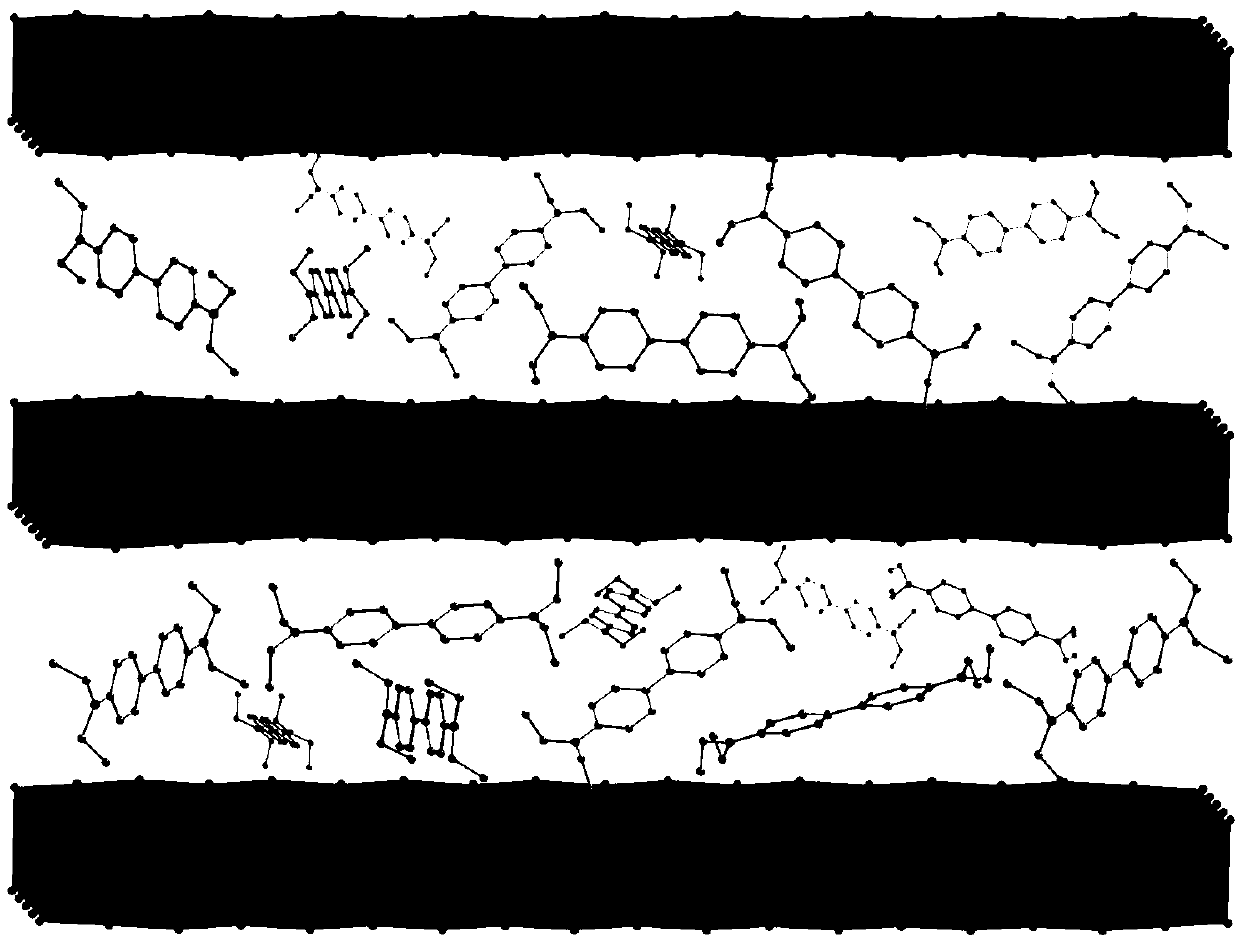
[0049] figure 1 Schematic diagram of the structure of the superlattice material prepared in Example 1. It includes EtDAB layer and PbI 2 layer, and the EtDAB layer with PbI 2 The layers are stacked alternately.
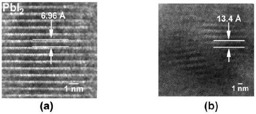
[0050] figure 2 For the transmission electron microscope figure of the superlattice material prepared by lead iodide and embodiment 1, from figure 2 The structure of the superlattice material is further confirmed in , wherein the thickness of the EtDAB layer is about The PbI 2 The...
Embodiment 2
[0053] Select the relatively large dark green sample sheet prepared in Example 1 (referred to as a synthetic sample), and under the protection of the mask, plate gold on both ends of the sheet, and use silver glue to lead electrodes on the gold. Put the electrode in the Lake Shore CRX-VF sample chamber to evacuate, and use KEITHLEY4200-SCS to test the voltage VS current curve at different temperatures to obtain the conductivity of the synthesized sample.
[0054] Then heat the sample prepared in the above Example 1 to 100°C for 2 hours to obtain a yellow sample, which is recorded as a heat-discolored sample; test the voltage VS current curve of the heat-discolored sample at different temperatures to obtain the heat-discolored sample conductivity.
[0055] The photoconductivity of the sample prepared in Example 1 above and its thermally discolored sample at different wavelengths was tested. Using the above-mentioned electrode preparation method, Xe lamp and laser are used as l...
PUM
| Property | Measurement | Unit |
|---|---|---|
| thickness | aaaaa | aaaaa |
| electrical conductivity | aaaaa | aaaaa |
| electrical conductivity | aaaaa | aaaaa |
Abstract
Description
Claims
Application Information
 - R&D
- Intellectual Property
- Life Sciences
- Materials
- Tech Scout
- Unparalleled Data Quality
- Higher Quality Content
- 60% Fewer Hallucinations
Browse by: Latest US Patents, China's latest patents, Technical Efficacy Thesaurus, Application Domain, Technology Topic, Popular Technical Reports.
© 2025 PatSnap. All rights reserved.Legal|Privacy policy|Modern Slavery Act Transparency Statement|Sitemap|About US| Contact US: help@patsnap.com


