Design method of plasma sensor and sensor prepared by design method

A plasma and design method technology, which is applied in nanotechnology, instruments, scientific instruments and other directions for sensing, can solve the problems of complex manufacturing process, difficult precision control, and cannot be reused, and achieves high parameter control precision and high Sensitivity and ease of mass production

Pending Publication Date: 2020-05-19
JINAN UNIVERSITY
View PDF4 Cites 1 Cited by
  • Summary
  • Abstract
  • Description
  • Claims
  • Application Information

AI Technical Summary

Problems solved by technology

[0005] The present invention aims at overcoming at least one defect (deficiency) of the above-mentioned prior art, and provides a design and preparation method of a plasma sensor, which avoids limited accuracy due to the

Method used


Image

  • Design method of plasma sensor and sensor prepared by design method
  • Design method of plasma sensor and sensor prepared by design method
  • Design method of plasma sensor and sensor prepared by design method

Examples


Embodiment 1

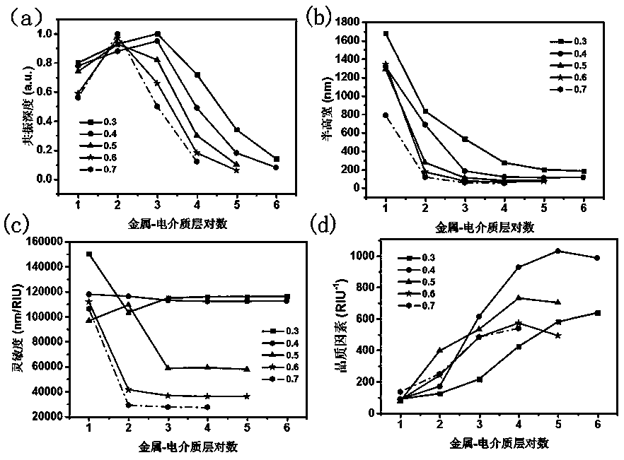
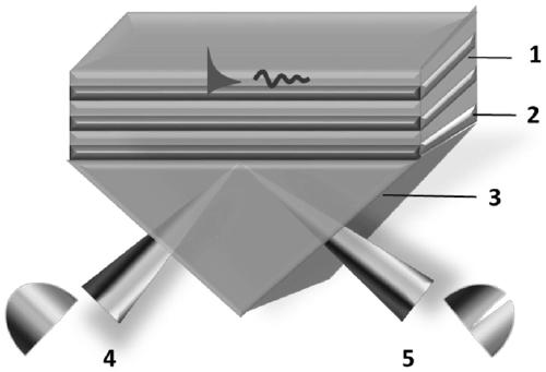
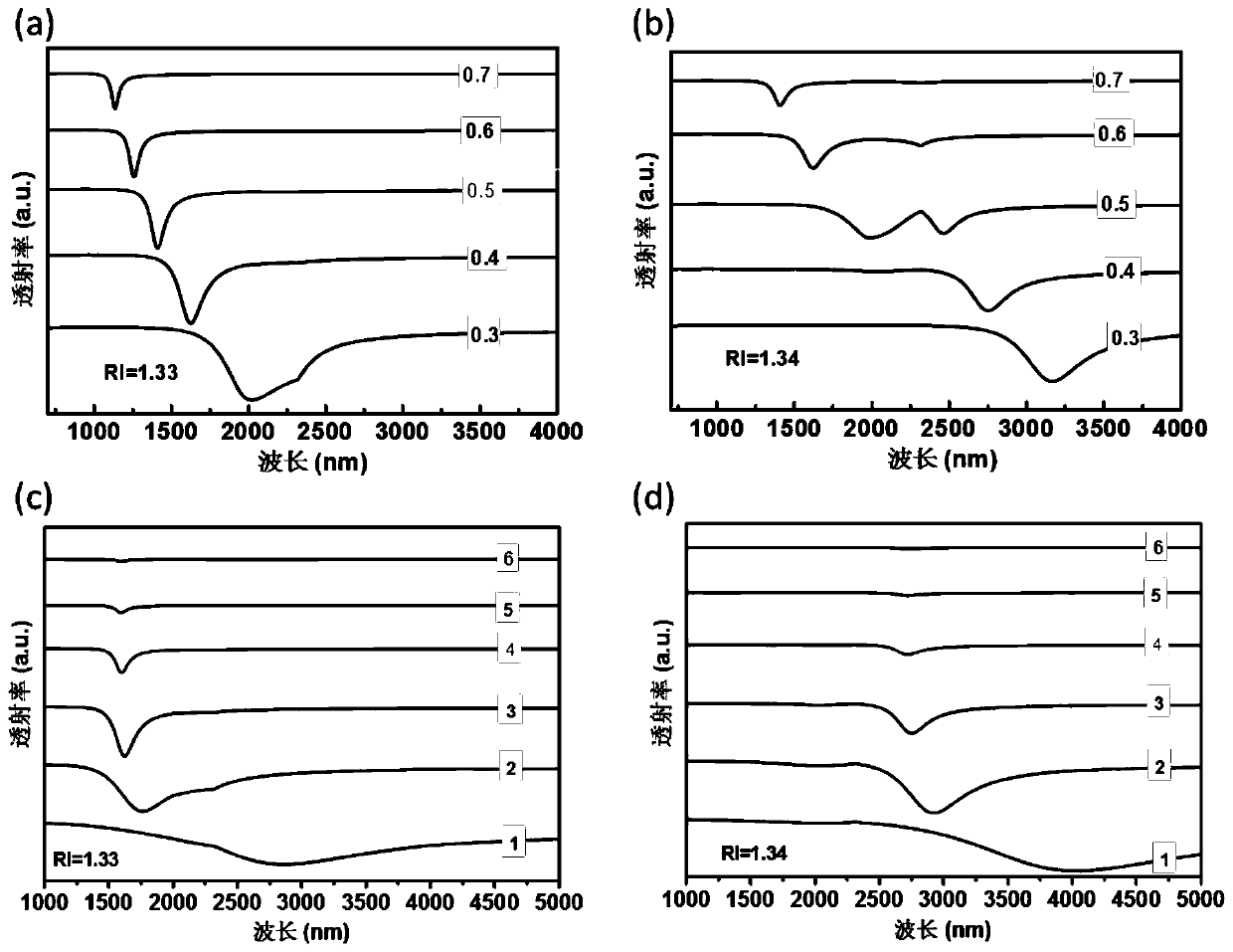
[0050] This embodiment provides a design method of a plasmonic sensor. Firstly, the metal filling ratio ρ of the hyperbolic metamaterial and the logarithm N of the metal-dielectric layer are obtained by software simulation calculation. bi The optimal combination parameters of the hyperbolic metamaterials are combined with the multilayer film structure of the optimal combination parameters and the Kretschmann structure to make a plasmon sensor. The sensor is a Kretschmann structure plasmon sensor based on the hyperbolic metamaterial dispersion engineering . Specifically, the metal in this embodiment is selected as Ag, and the dielectric is TiO 2 ,like figure 1 Shown is the principle structure diagram of the Kretschmann structure plasmon sensor based on hyperbolic metamaterial dispersion engineering in this embodiment, wherein the serial numbers represent: 1, titanium dioxide; 2, silver; 3, prism; 4, incident light; 5, outgoing light.

[0051] Furthermore, the simulation proc...

Embodiment 2

[0064] In the design method of a plasmonic sensor provided in this embodiment, the metal filling ratio ρ of the hyperbolic metamaterial and the logarithm N of the metal-dielectric layer are calculated first. bi The optimal combination parameters of the hyperbolic metamaterials are combined with the multilayer film structure of the optimal combination parameters and the polishing surface of the side-polished optical fiber to make a plasmonic sensor. The obtained sensor is based on the hyperbolic metamaterial dispersion The side polished fiber optic plasma sensor of the project, its principle and cross-sectional diagram are as follows Figure 5 shown.

[0065] Further, the simulation process uses the finite element method, and uses the quality factor FOM as a reference value to optimize the simulation to obtain the best hyperbolic metamaterial parameter combination. The sensor is a side-polished optical fiber based on hyperbolic metamaterial dispersion engineering. Structured p...


PUM

PropertyMeasurementUnit
Thicknessaaaaaaaaaa
Thicknessaaaaaaaaaa
Thicknessaaaaaaaaaa

Abstract

The invention discloses a design method of a plasma sensor and a sensor prepared by the design method. The method comprises the following steps: firstly, utilizing software simulation calculation to obtain optimal combination parameters of a metal filling ratio rho of a hyperbolic metamaterial and a logarithm Nbi of a metal-dielectric layer; and then combining the hyperbolic metamaterial with a polishing surface of a Kretschmann structure or a side polishing optical fiber by a multilayer film structure with the optimal combination parameters to manufacture a corresponding plasma sensor. Compared with the prior art, the design method provided by the invention has the advantages that the performance parameters of the sensor can be controlled by regulating and controlling the metal filling ratio (rho) of the hyperbolic metamaterial and the logarithm (Nbi) of the metal-dielectric layer, so that the controllability of the performance parameters is realized; the plasma sensor prepared by themethod has the advantages of adjustable wavelength, high sensitivity, high quality factor (FOM), simple manufacturing and the like, and is far better than an existing plasma sensor.

Description

technical field [0001] The invention relates to the technical field of preparation of plasma sensors, and more particularly, relates to a design of a plasma sensor and a sensor thereof. Background technique [0002] In recent years, due to the advantages of high sensitivity, good real-time performance, and label-free detection, plasmonic sensors have received important research in the fields of medical detection, food safety, drug screening, and environmental detection. For a given angle of incidence, when the wave vectors of the incident light wave and the plasmon wave match, plasmon resonance occurs at a resonant wavelength that is very sensitive to changes in the surrounding refractive index (SRI). However, there are still challenges in the detection of small molecules with ultra-low concentrations or molecular weights less than 500Da. In order to solve this problem, many methods to improve the performance of the sensor have been proposed, for example, adding a dielectri...

Claims


Application Information

Patent Timeline
IPC IPC(8): G01N21/25G01N27/62B82Y15/00B82Y40/00
CPCG01N21/25G01N27/62B82Y15/00B82Y40/00G01N2021/258
Inventor 罗云瀚胡诗琦陈耀飞刘贵师陈哲陈宇施伟成陈雷
Owner JINAN UNIVERSITY
Why Eureka
Try Eureka