Vertical GaN Schottky device structure with high breakdown voltage and low reverse electric leakage

A high breakdown voltage, reverse leakage technology, applied in electrical components, semiconductor devices, circuits, etc., can solve the difficulty of doping the second conductivity type, the reduction of the forward current density of the device, and the low activation rate of P+ ions, etc. problems, to achieve the effect of reducing leakage current, reducing reverse leakage current, and overcoming the low activation rate of impurities

Active Publication Date: 2020-05-22
XI AN JIAOTONG UNIV
View PDF5 Cites 6 Cited by
  • Summary
  • Abstract
  • Description
  • Claims
  • Application Information

AI Technical Summary

Problems solved by technology

[0004] However, when a large reverse bias voltage is applied to the vertical GaN Schottky power device, the Schottky junction withstand voltage rises rapidly, and the Schottky barrier will be reduced due to the image force, and its reverse breakdown voltage is relatively lower, larger reverse leakage current
[0005] In order to increase the breakdown voltage of vertical GaN Schottky devices, it is generally necessary to increase the thickness of the low-doped GaN layer of the first conductivity type. In order to reduce the reverse leakage current of vertical GaN Schottky devices, a P+ injection region is introduced The vertical GaN Schottky device structure has been proposed. Due to the difficulty of doping the second conductivity type of GaN material, the activation rate of P+ ions is low, which makes the forward current density of the device smaller.

Method used


Image

  • Vertical GaN Schottky device structure with high breakdown voltage and low reverse electric leakage
  • Vertical GaN Schottky device structure with high breakdown voltage and low reverse electric leakage
  • Vertical GaN Schottky device structure with high breakdown voltage and low reverse electric leakage

Examples


Embodiment Construction

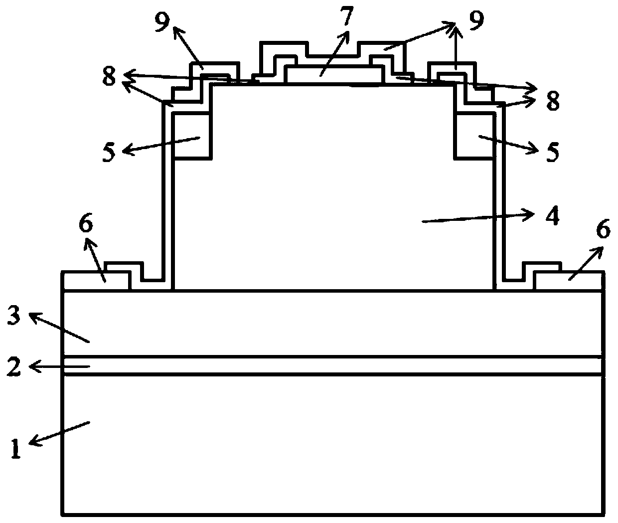
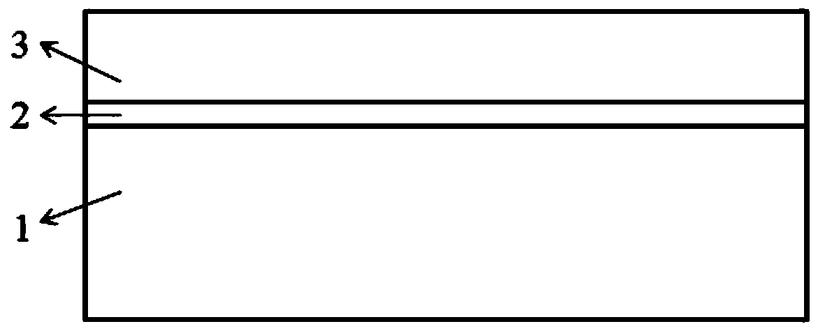
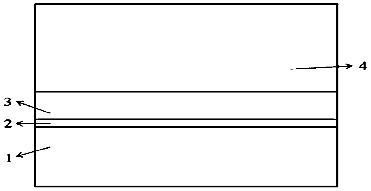
[0039]In describing the present invention, it should be understood that the terms "center", "longitudinal", "transverse", "upper", "lower", "front", "rear", "left", "right", " The orientation or positional relationship indicated by "vertical", "horizontal", "top", "bottom", "inner", "outer", "side", "end", "side" etc. is based on the Orientation or positional relationship is only for the convenience of describing the present invention and simplifying the description, and does not indicate or imply that the referred device or element must have a specific orientation, be constructed and operated in a specific orientation, and thus should not be construed as a limitation of the present invention. In addition, the terms "first" and "second" are used for descriptive purposes only, and cannot be interpreted as indicating or implying relative importance or implicitly specifying the quantity of indicated technical features. Thus, a feature defined as "first" and "second" may explicitl...


PUM

PropertyMeasurementUnit
thicknessaaaaaaaaaa
thicknessaaaaaaaaaa
thicknessaaaaaaaaaa

Abstract

The invention discloses a vertical GaN Schottky device structure with high breakdown voltage and low reverse electric leakage. The vertical GaN Schottky device structure comprises a first conductive type highly-doped GaN layer, a first conductive type low-doped GaN layer, a second conductive type NiO filling layer, a SiO2 and Si3N4 mixed dielectric layer, a floating metal field plate, an ohmic cathode, a Schottky anode, a sapphire substrate and an AlN nucleating layer. According to the device structure provided by the invention, a two-step etching process is applied, so that the operability problem of a deep etching technology is solved; the designed second conductive type NiO filling layer overcomes the technical problem of second conductive type doping of a GaN material, effectively shields a high electric field and protects a Schottky barrier, so that the reverse leakage current of the device is effectively reduced; the designed multi-field-plate structure effectively utilizes the advantage of high field plate contact area brought by a two-step etching process, weakens the fringe field concentration effect of the device, and effectively improves the reverse breakdown voltage ofthe device.

Description

technical field [0001] The invention belongs to the technical field of microelectronic gallium nitride power devices, and in particular relates to a vertical GaN Schottky device structure with high breakdown voltage and low reverse leakage. Background technique [0002] Wide bandgap semiconductor GaN materials have excellent physical properties such as high breakdown field strength, high electron saturation drift rate, and low dielectric constant, making GaN power semiconductor devices quickly become the first choice for electronic equipment in the high-frequency and high-power field. [0003] In GaN Schottky power devices, the lateral structure device must increase the cathode distance proportionally to increase the breakdown voltage, resulting in an increase in device size and a greatly increased manufacturing cost; in addition, when the device transmits a large current, there will be a self-heating effect, Seriously affect the stability of the device. The GaN-based verti...

Claims


Application Information

Patent Timeline
Patent Type & Authority Applications(China)
IPC IPC(8): H01L29/872H01L29/40
CPCH01L29/872H01L29/404
Inventor 耿莉刘成杨明超刘江李安鸽刘卫华郝跃张勇
Owner XI AN JIAOTONG UNIV
Why Eureka
Try Eureka