Method for preparing large-area beta-phase indium selenide single crystal film

A single-crystal thin-film, large-area technology, applied in semiconductor/solid-state device manufacturing, electrical components, circuits, etc., can solve the problems of impurity phase, low crystal quality, small film area, etc.

Active Publication Date: 2020-05-29
UNIV OF ELECTRONICS SCI & TECH OF CHINA
View PDF8 Cites 0 Cited by
  • Summary
  • Abstract
  • Description
  • Claims
  • Application Information

AI Technical Summary

Problems solved by technology

[0010] Preparation of β-In for current growth 2 Se 3 In the thin film technology, the film area is small, the crystal quality is not high, and there are many problems such as impurities. The present invention provides a ...

Method used


Image

  • Method for preparing large-area beta-phase indium selenide single crystal film
  • Method for preparing large-area beta-phase indium selenide single crystal film
  • Method for preparing large-area beta-phase indium selenide single crystal film

Examples


Embodiment 1

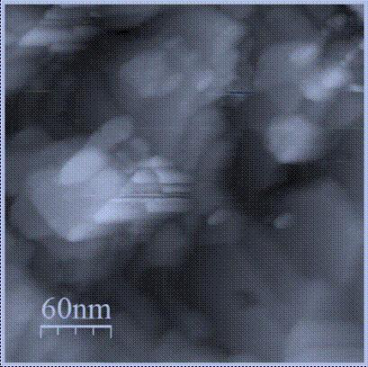
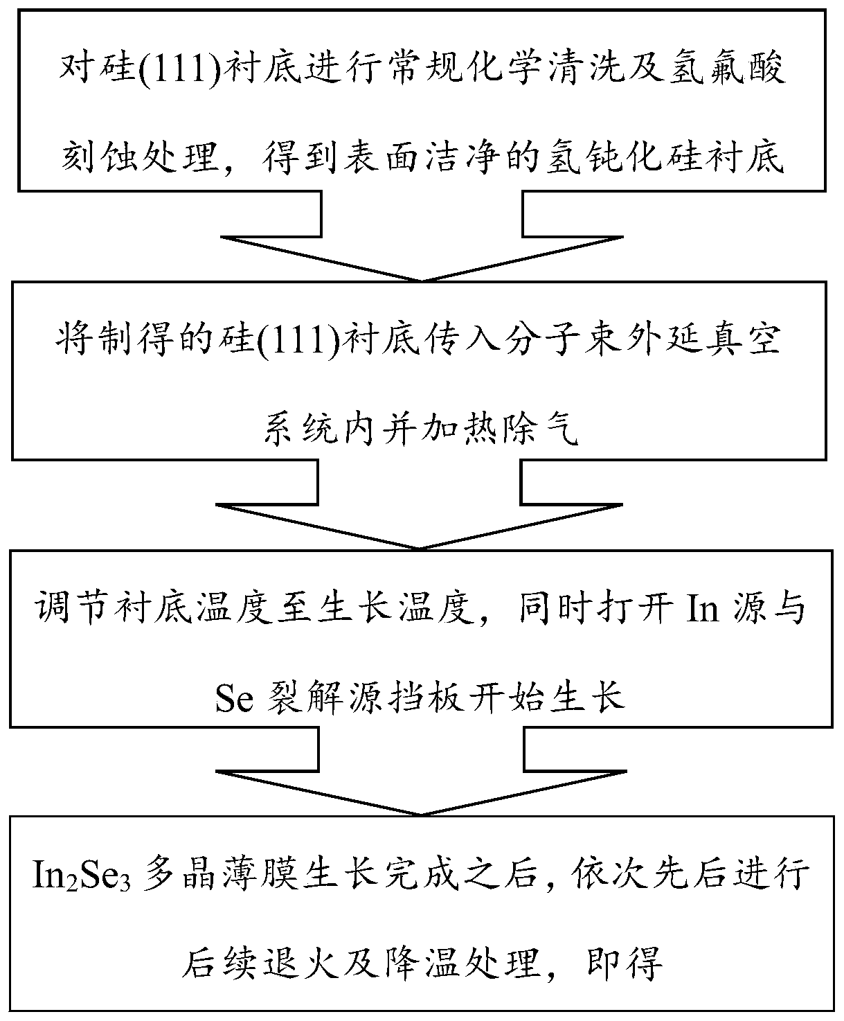
[0035] Such as figure 1 As shown, the present invention is a method for growing large-area high-quality β-phase single crystal In on a silicon substrate. 2 Se 3 The method for thin film specifically comprises the following steps:

[0036] 1): The silicon (111) substrate is placed before the ultra-high vacuum molecular beam epitaxy system, and the single crystal silicon substrate is chemically cleaned and chemically etched to obtain a flat silicon substrate with clean surface and hydrogen passivation. In the example, Acetone ultrasonic cleaning was performed for 3 minutes, alcohol ultrasonic cleaning was performed for 3 minutes, and ultrasonic cleaning was repeated for 3 rounds; then the substrate surface was chemically etched with 49% hydrofluoric acid solution for 1 minute.

[0037] 2): Put the silicon substrate prepared in step 1) into the molecular beam epitaxy vacuum system and heat it for degassing. When the maximum degassing temperature is 180°C, stop heating and degas...

Embodiment 2

[0049] The invention is a low-temperature growth of large-area single-crystal β-phase In on a silicon substrate. 2 Se 3 The method for thin film specifically comprises the following steps:

[0050] 1): Chemically clean the monocrystalline silicon (111) substrate and passivate the surface layer with hydrofluoric acid to obtain a flat silicon substrate with a clean surface. In the example, use acetone ultrasonic cleaning for 4 minutes, alcohol ultrasonic cleaning for 4 minutes, and repeat ultrasonic cleaning. Cleaning for 3 rounds; then corroding the substrate with a hydrogen fluoride reagent with a concentration of 49% for 2 minutes, then cleaning the residual chemical reagents on the surface with high-purity water, and then drying with high-purity nitrogen.

[0051] 2): Put the silicon substrate prepared in step 1) into the molecular beam epitaxy vacuum system and heat it for degassing. When the maximum degassing temperature is 180°C, stop heating and degas until the pressure...


PUM

PropertyMeasurementUnit
Surface roughnessaaaaaaaaaa

Abstract

The invention relates to a method for preparing a large-area beta-phase In2Se3 single crystal film. The method comprises the following steps that: 1) chemical cleaning and chemical corrosion treatmentare carried out on a silicon substrate with crystal orientation of (111), so that a hydrogen-passivated silicon substrate with a clean surface can be obtained; 2) the prepared silicon substrate is transferred into a molecular beam epitaxy system, heating is performed to 180 DEG C, and degassing is performed until the vacuum degree of the system is superior to 8*10 <-10 > mbar; (3) the substrate naturally cools to a growth temperature range after the substrate is degassed, and meanwhile, an In beam source and a Se beam source are opened to grow and synthesize an In2Se3 polycrystalline film; (4) the temperature of the substrate is immediately raised to 300-350 DEG C after the growth of the polycrystalline film is finished, and subsequent annealing is carried out for 5 minutes; and 5) heating is immediately stopped after annealing is finished, and the substrate naturally cools to room temperature, so that a high-quality beta-phase In2Se3 single crystal film can be obtained. According tothe method for growing the beta-phase In2Se3 thin film, the molecular beam epitaxy technology is combined with the subsequent in-situ annealing process, and the large-area high-quality beta-phase In2Se3 single crystal thin film can be prepared on the hydrogen-passivated silicon substrate at a low temperature.

Description

technical field [0001] The invention belongs to the field of semiconductor materials, and specifically relates to a method for preparing a large-area β-phase indium selenide single crystal thin film, in particular, using molecular beam epitaxy technology combined with a subsequent in-situ annealing process on a hydrogen passivated silicon (111) substrate A method for preparing high-quality β-phase indium selenide single crystal thin film materials by growing at a lower temperature. Background technique [0002] Indium selenide (chemical formula: In 2 Se 3 ) is an important class of direct bandgap semiconductor materials in the III-VI system, with five main crystal phases of α, β, γ, δ and κ. Among them, the β-phase indium selenide whose crystal space group is 3R (hereinafter referred to as β-In 2 Se 3 ) is in a metastable state at normal temperature and pressure, and has the lowest resistivity among the five known indium selenide crystal phases. Due to the metastable β-...

Claims


Application Information

Patent Timeline
IPC IPC(8): H01L21/02
CPCH01L21/0256H01L21/02598H01L21/02612H01L21/02664Y02P70/50
Inventor 李含冬贺靖尹锡波徐超凡李俊烨姬海宁牛晓滨王志明
Owner UNIV OF ELECTRONICS SCI & TECH OF CHINA
Why Eureka
Try Eureka