Multi-junction solar cell and preparation method thereof
A solar cell and battery technology, applied in circuits, photovoltaic power generation, electrical components, etc., can solve problems such as mismatch between tunnel junctions and sub-cells, and achieve the effects of improving tunneling effect, reducing process difficulty, and reducing doping defects
- Summary
- Abstract
- Description
- Claims
- Application Information
AI Technical Summary
Problems solved by technology
Method used
Image

Examples
preparation example Construction
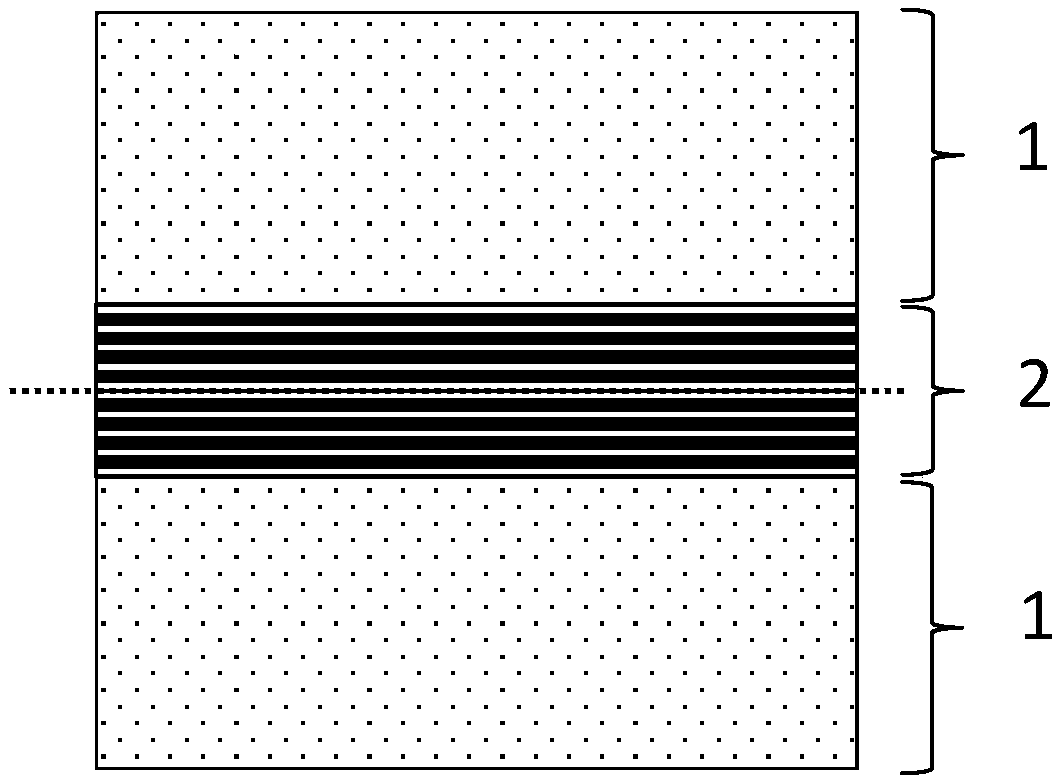
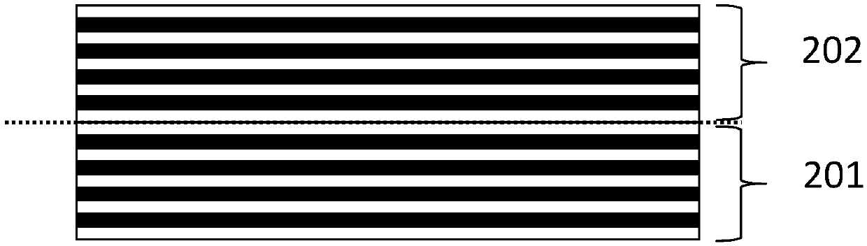
[0034] According to another aspect of the present invention, there is also provided a method for preparing the above-mentioned multi-junction solar cell, including the step of forming a tunnel junction layer 2: forming an N-type semiconductor layer 201 and a P-type semiconductor layer 202 on the sub-cell 1, The N-type semiconductor layer 201 is located on the side of the sub-cell 1 away from the P-type semiconductor layer 202, or the P-type semiconductor layer 202 is located on the side of the sub-cell 1 away from the N-type semiconductor layer 201, and the obtained multi-junction solar cell is as follows Figure 1 to Figure 3 shown.
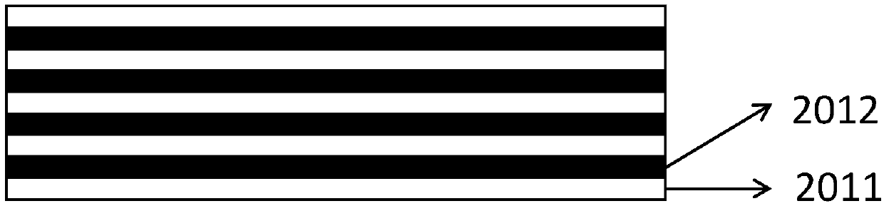
[0035] In a preferred embodiment, the step of forming the above-mentioned N-type semiconductor layer 201 and the step of forming the above-mentioned P-type semiconductor layer 202 independently include: alternately forming stacked first-type doped layers 2011 and second-type doped layers on the sub-cell 1 The second type doped layer 2012, the fi...
Embodiment 1
[0056] This embodiment provides a method for preparing a GaAs / GaInP double-junction solar cell, wherein an epitaxial growth substrate is used, and the epitaxial layer includes: a p-GaInP back field layer, a P-GaAs base layer, an n-GaInAs emission layer, n - AlGaAs window layer, n++GaAs / p++AlGaAs tunnel junction, p-AlGaInP back field layer, p-GaInP base region, n-GaInP emitter layer, n-AlInP window layer and n++GaInAs contact layer.
[0057] Above-mentioned preparation method comprises the following steps:
[0058] 1) Pass the Si substrate into the MOCVD equipment, pass through the H 2 Gas, raise the temperature to perform high-temperature cleaning on the substrate, the temperature is 600°C.
[0059] 2) Al growth on the substrate X Ga 1-X The As back field layer, where x takes a value of 0.5, y takes a value of 0.5, a thickness of 100nm, and a growth temperature of 800°C.
[0060] 3) A GaAs base layer is grown on the back field layer with a thickness of 2500nm and a growth ...
Embodiment 2
[0071] The difference between this embodiment and embodiment 1 is:
[0072] In step 6), the doping concentration of the formed first-type doped layer is 0, and the doping concentration of the second-type doped layer is 1E19.
PUM
| Property | Measurement | Unit |
|---|---|---|
| Thickness | aaaaa | aaaaa |
Abstract
Description
Claims
Application Information
 - Generate Ideas
- Intellectual Property
- Life Sciences
- Materials
- Tech Scout
- Unparalleled Data Quality
- Higher Quality Content
- 60% Fewer Hallucinations
Browse by: Latest US Patents, China's latest patents, Technical Efficacy Thesaurus, Application Domain, Technology Topic, Popular Technical Reports.
© 2025 PatSnap. All rights reserved.Legal|Privacy policy|Modern Slavery Act Transparency Statement|Sitemap|About US| Contact US: help@patsnap.com