Gallium nitride power device with multi-field plate structure, and preparation method thereof

A technology of power devices and gallium nitride, which is applied in semiconductor/solid-state device manufacturing, semiconductor devices, electrical components, etc., can solve problems such as limited effects, device performance degradation, and serious reliability of traditional devices, so as to achieve enhanced withstand voltage, Effects of improving reliability and suppressing current collapse effect

Active Publication Date: 2020-07-03
CHANGSHU INSTITUTE OF TECHNOLOGY
View PDF4 Cites 7 Cited by
  • Summary
  • Abstract
  • Description
  • Claims
  • Application Information

AI Technical Summary

Problems solved by technology

[0004] At the same time, existing studies have shown that there is a large electric field peak at the end of the gate of the HEMT device when it is working. In the working state of the device, the strong electric field at the end of the gate will cause a large number of interface states in this region, resulting in a decline in device performance. raises reliability issues
At present, the solution to this problem is to increase the gate field plate to shield the strong electric field at the end of the device gate. However, the effect of the traditional gate field plate is limited, and there will still be a strong electric field at the end of the device gate, so that the traditional device is still There are serious reliability problems

Method used


Image

  • Gallium nitride power device with multi-field plate structure, and preparation method thereof
  • Gallium nitride power device with multi-field plate structure, and preparation method thereof

Examples


Embodiment 1

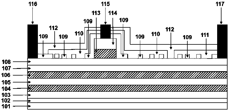
[0047] Example 1, such as figure 1 As shown, a GaN power device with high reliability involved in this embodiment includes a silicon substrate 101 arranged in sequence from bottom to top, an AlN nucleation layer 102 with a thickness of 5 nm, a GaN buffer layer 103 with a thickness of 1000 nm, The GaN / AlInN first insertion layer 104 has a period number of 5 and a thickness of 50nm; the first GaN layer 105 has a thickness of 1000nm; the AlN second insertion layer 106 has a thickness of 10nm; 5nm thick, SiO 2 Passivation layer 109 with a thickness of 20nm, titanium / aluminum / nickel / gold gate field plate 110, titanium / aluminum / nickel / gold drain field plate 111, Si 3 N 4 The protective layer 112 has a thickness of 200 nm, and the p-type doping concentration of the GaN / AlInGaN gate insertion layer 113 is: 1×10 16 cm -3 , the number of periods is 1, the thickness is 5nm, and the doping concentration of the p-type GaN gate 114 is: 1×10 16 cm -3 , with a thickness of 30 nm, titani...

Embodiment 2

[0071] Example 2, such as figure 1As shown, a GaN power device with high reliability involved in this embodiment includes a silicon substrate 101 arranged in sequence from bottom to top, an AlN nucleation layer 102 with a thickness of 15 nm, a GaN buffer layer 103 with a thickness of 1500 nm, The GaN / AlInN first insertion layer 104 has a period number of 15 and a thickness of 400nm, the first GaN layer 105 has a thickness of 1500nm, the AlN second insertion layer 106 has a thickness of 70nm, the second GaN layer 107 has a thickness of 1500nm, and the AlGaN barrier layer 108 Thickness 35nm, SiO 2 Passivation layer 109 with a thickness of 150nm, titanium / aluminum / nickel / gold gate field plate 110, titanium / aluminum / nickel / gold drain field plate 111, Si 3 N 4 The protective layer 112 has a thickness of 1500 nm, and the p-type doping concentration of the GaN / AlInGaN gate insertion layer 113 is: 1×10 18 cm -3 , the number of periods is 3, the thickness is 35nm, and the doping co...

Embodiment 3

[0077] Embodiment 3, a gallium nitride power device with high reliability involved in this embodiment, including a sapphire substrate arranged in sequence from bottom to top, an AlN nucleation layer with a thickness of 20nm, a GaN buffer The thickness of the layer is 3000nm, the period number of the first GaN / AlInGaN insertion layer is 20, the thickness is 500nm, the thickness of the first GaN layer is 3000nm, the thickness of the second insertion layer of AlN / AlInGaN is 100nm, the thickness of the second GaN layer 107 is 3000nm, AlGaN The thickness of the barrier layer is 50nm, Si 3 N 4 Passivation layer thickness 200nm, Ti / Al / Ni gate field plate, Ti / Al / Ni drain field plate, SiO 2 The thickness of the protective layer is 2000nm, and the p-type doping concentration of the AlInGaN gate insertion layer is: 1×10 21 cm -3 , the thickness is 50nm, the p-type GaN gate doping concentration is: 1×10 21 cm -3 , a thickness of 100nm, titanium / aluminum / nickel gate metal, titanium / al...


PUM

PropertyMeasurementUnit
thicknessaaaaaaaaaa
thicknessaaaaaaaaaa
thicknessaaaaaaaaaa

Abstract

The invention discloses a gallium nitride power device with a multi-field plate structure. The gallium nitride power device is sequentially provided with a substrate, a nucleating layer, a buffer layer, a first insertion layer, a first GaN layer, a second insertion layer, a second GaN layer, an AlGaN barrier layer, a passivation layer, a grid electrode field plate, a drain electrode field plate, aprotective layer, a grid electrode insertion layer, a p-type GaN grid electrode, a grid electrode metal, a source electrode metal and a drain electrode metal from bottom to top, wherein the passivation layer located on the surface of the AlGaN barrier layer is in a strip shape arranged at intervals, the grid electrode field plate and the drain electrode field plate respectively cover part of thepassivation layer, and the surfaces of the grid electrode field plate and the drain electrode field plate and the space between the grid electrode field plate and the drain electrode field plate are covered with the protective layer. According to the invention, the electric field distribution is uniform, the voltage endurance capability of the device is enhanced, the stability of grid electrode turn-on voltage and grid electrode voltage of the device is effectively improved, and the electric leakage of the device under the action of large current is effectively reduced. The preparation methodis completely compatible with a traditional process, and the preparation difficulty is low.

Description

technical field [0001] The invention relates to a gallium nitride power device and a preparation method thereof, in particular to a gallium nitride power device with a multi-field plate structure and a preparation method thereof. Background technique [0002] High electron mobility transistors (HEMTs) based on gallium nitride materials have the advantages of high breakdown voltage, high electron mobility, fast switching speed, and simple process steps, and have broad application prospects in the field of power semiconductor devices. However, HEMT devices will be subjected to high-intensity electric field stress in the working state, which will cause interface damage during the long-term operation of the device, which will degrade the performance of the device or even damage it. Therefore, improving the reliability of devices through design is an important issue concerned by device designers. [0003] In terms of epitaxial material growth, due to the huge lattice mismatch an...

Claims


Application Information

Patent Timeline
Patent Type & Authority Applications(China)
IPC IPC(8): H01L29/778H01L29/06H01L29/15H01L29/40H01L29/423H01L21/335
CPCH01L29/778H01L29/15H01L29/404H01L29/0607H01L29/42316H01L29/66462Y02B70/10
Inventor 王书昶穆久涛冯源况亚伟张惠国
Owner CHANGSHU INSTITUTE OF TECHNOLOGY
Why Eureka
Try Eureka