Diamond film preparing device and method

A diamond film and film-forming technology, which is applied in metal material coating process, gaseous chemical plating, coating, etc., can solve the problems of poor uniformity of diamond film thickness, difficult diamond film polishing process, diamond waste, etc.

Pending Publication Date: 2020-07-07
SHANGHAI ZHENGSHI TECH CO LTD
View PDF5 Cites 10 Cited by
  • Summary
  • Abstract
  • Description
  • Claims
  • Application Information

AI Technical Summary

Problems solved by technology

Because the microwave energy above the spin-rotating substrate stage in the middle area of ​​the plasma reaction chamber is the strongest, the energy density distribution in the plasma ball is different, so the thickness uniformity of the large-area diamond film grown is

Method used


Image

  • Diamond film preparing device and method
  • Diamond film preparing device and method
  • Diamond film preparing device and method

Examples


Embodiment 1

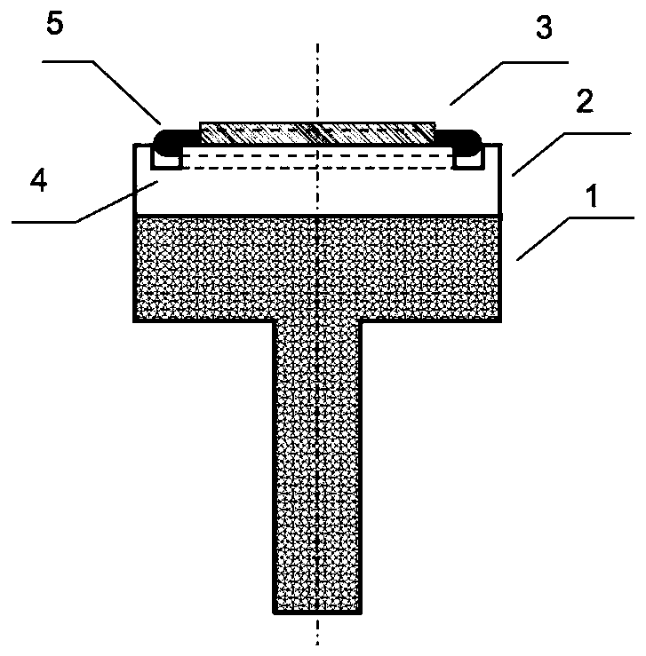
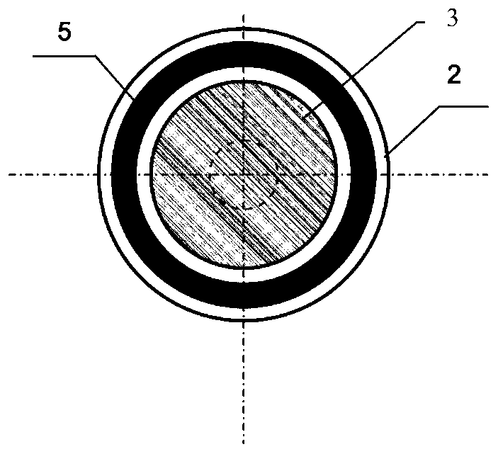
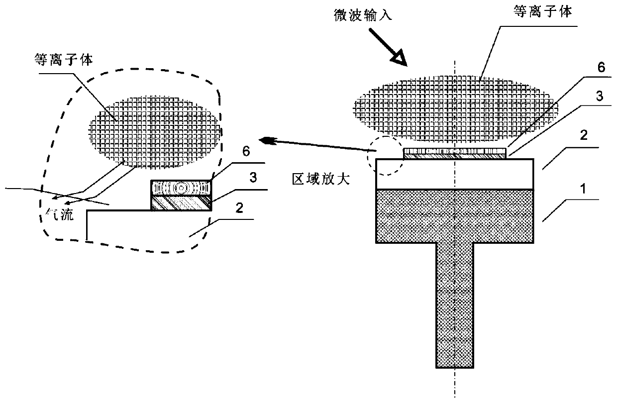
[0048] The substrate material is a circular metal molybdenum plate with a diameter of 60mm and a thickness of 4.0mm. The outer diameter of the annular pit on the surface is 57mm, the width is 3.0mm, and the depth is 1.0mm. The filler metal is Fe wire with a diameter of 3.0mm. Put the molybdenum plate and Fe wire together in an acetone solution for 10 minutes of ultrasonication, take out the dustproof and dry it to get a clean substrate material.

[0049] The diamond film was deposited on a P-type (100) single crystal silicon wafer with a diameter of 50 mm and a thickness of 0.2 mm as the film-forming base material. Grind the silicon chip with diamond powder with a particle size of 100nm for 15 minutes on a grinding disc, then ultrasonicate it in an acetone solution containing a small amount of 100nm diamond powder for 5 minutes, rinse it in acetone for 5 minutes, and dry it with absorbent cotton to obtain a surface degreasing treatment. film-forming substrate material.

[005...

Embodiment 2

[0062] The substrate material is a circular metal molybdenum plate with a diameter of 30mm and a thickness of 4.0mm. The outer diameter of the annular pit on the surface is 28mm, the width is 2.0mm, and the depth is 1.0mm. The filler metal is Ni wire with a diameter of 2.0mm. Put the molybdenum plate and Ni wire together in the acetone solution for 10 minutes of ultrasonication, take out the dustproof and dry it to get a clean substrate material.

[0063] The diamond film was deposited on a P-type (100) single crystal silicon wafer with a diameter of 25 mm and a thickness of 0.2 mm as the film-forming base material. Grind the silicon chip with diamond powder with a particle size of 100nm for 15 minutes on a grinding disc, then ultrasonicate it in an acetone solution containing a small amount of 100nm diamond powder for 5 minutes, rinse it in acetone for 5 minutes, and dry it with absorbent cotton to obtain a surface degreasing treatment. film-forming substrate material.

[00...


PUM

PropertyMeasurementUnit
Diameteraaaaaaaaaa
Thicknessaaaaaaaaaa
Outer diameteraaaaaaaaaa

Abstract

The invention provides a diamond film preparing device and method. The preparing device adopts a microwave plasma chemical vapor deposition device which comprises a microwave system, a vacuum system,a gas supply system and a plasma reaction chamber, wherein a self-rotating substrate table is arranged in the plasma reaction chamber, microwaves generated by the microwave system enter the plasma reaction chamber in the working process, gas provided by the gas supply system is excited above the self-rotating substrate table to generate plasma balls, a substrate material is arranged on the self-rotating substrate table, an annular pit is formed in the position, close to the outer edge, of the substrate material, the pit is filled with a metal material, and the metal material is higher than thesurface of the substrate material to form an annular metal protrusion. The preparing device and method have the advantages that the substrate material is improved, so that the surface of the film-forming substrate material has relatively proper air flow distribution and plasma distribution when a diamond film is deposited.

Description

technical field [0001] The invention belongs to the technical field of vacuum microelectronics, and in particular relates to a device for preparing a diamond film and a method for preparing a diamond film using the device. Background technique [0002] Diamond has extremely high hardness, and has excellent properties such as extremely high thermal conductivity, low expansion coefficient, and high chemical inertness at room temperature. It can be used to make cutting tools and wear-resistant parts, and is widely used in the field of mechanical processing. In addition, it is also an ideal material for making surface pressure sensors, radiation-resistant semiconductor devices, high-power semiconductor laser-level high-density anti-corrosion and wear-resistant infrared optical windows and other devices. However, natural diamonds are scarce, expensive and difficult to process, which restricts the widespread use of diamonds. The diamond synthesized by the high temperature and hig...

Claims


Application Information

Patent Timeline
IPC IPC(8): C23C16/27C23C16/458C23C16/511C23C16/513C23C16/517
CPCC23C16/274C23C16/276C23C16/4584
Inventor 龚闯满卫东吴剑波
Owner SHANGHAI ZHENGSHI TECH CO LTD
Why Eureka
Try Eureka