Post-processing method of quantum dot light-emitting diode

A quantum dot light-emitting and diode technology, which is applied in semiconductor devices, electrical components, circuits, etc., can solve the problems of long post-processing methods and insignificant effect of quantum dot light-emitting diode devices, so as to shorten the production cycle and improve the device's luminescence. Efficiency, the effect of good device luminous efficiency

Active Publication Date: 2021-07-02
TCL CORPORATION
View PDF5 Cites 0 Cited by
  • Summary
  • Abstract
  • Description
  • Claims
  • Application Information

AI Technical Summary

Problems solved by technology

[0004] The purpose of the present invention is to provide a post-processing method for quantum dot light-emitting diodes, which aims to solve the problem that the existing post-processing method of quantum dot light-emitting diodes takes too long and has no obvious effect on improving the efficiency of quantum dot light-emitting diodes.

Method used


Image

  • Post-processing method of quantum dot light-emitting diode
  • Post-processing method of quantum dot light-emitting diode
  • Post-processing method of quantum dot light-emitting diode

Examples


Embodiment 1

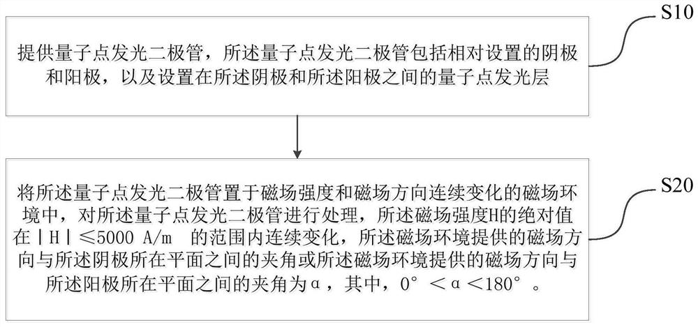
[0041] A post-processing method for quantum dot light-emitting diodes, comprising the following steps:

[0042] Quantum dot light-emitting diodes are provided, and the quantum dot light-emitting diodes include an anode (ITO) and a cathode (metal aluminum electrode) arranged oppositely, a functional stack structure arranged between the anode and the cathode, and the functional stack The structure includes a hole injection layer (PEDOT:PSS), a hole transport layer (TFB), a quantum dot light-emitting layer (CdSe / ZnS QDs), an electron transport layer (ZnO), and an electron injection layer stacked in sequence from the anode to the cathode. layer (LiF), wherein the anode is disposed on a glass substrate.

[0043] The quantum dot light-emitting diode is placed in a magnetic field environment, so that the angle α between the direction of the magnetic field provided by the magnetic field environment and the cathode or between the anode and the anode is 90°, and the magnetic field stren...

Embodiment 2

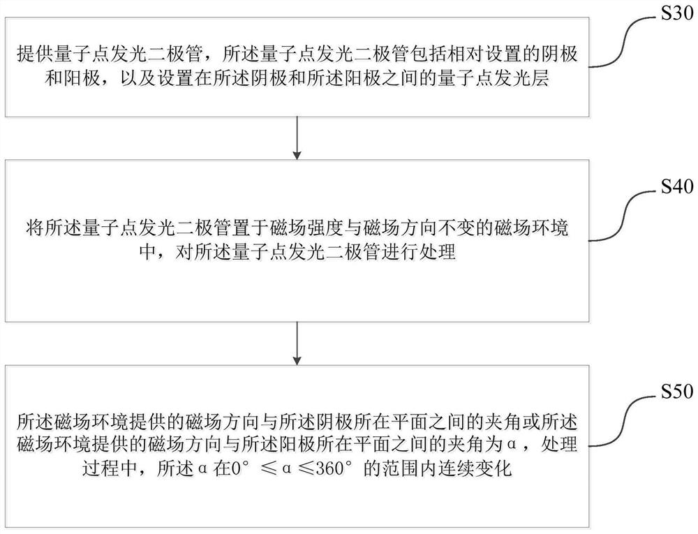
[0045] A post-processing method for quantum dot light-emitting diodes, comprising the following steps:

[0046] Quantum dot light-emitting diodes are provided, and the quantum dot light-emitting diodes include an anode (ITO) and a cathode (metal aluminum electrode) arranged oppositely, a functional stack structure arranged between the anode and the cathode, and the functional stack The structure includes a hole injection layer (PEDOT:PSS), a hole transport layer (TFB), a quantum dot light emitting layer (CdSe / ZnS QDs), an electron transport layer (ZnO), and an electron injection layer stacked in sequence from the anode to the cathode. layer (LiF), wherein the anode is disposed on a glass substrate.

[0047] The quantum dot light-emitting diode is placed in a magnetic field environment, so that the angle α between the direction of the magnetic field provided by the magnetic field environment and the cathode or between the anode changes sinusoidally between 0° and 180°, and the ...


PUM

PropertyMeasurementUnit
thicknessaaaaaaaaaa
thicknessaaaaaaaaaa
thicknessaaaaaaaaaa

Abstract

The invention provides a post-processing method of a quantum dot light-emitting diode, comprising the following steps: providing a quantum dot light-emitting diode, the quantum dot light-emitting diode includes a cathode and an anode oppositely arranged, and an anode arranged between the cathode and the anode The quantum dot light-emitting layer between them; the quantum dot light-emitting diode is placed in a magnetic field environment where the magnetic field strength and the direction of the magnetic field change continuously, and the absolute value of the magnetic field strength H is continuous within the range of 0A / m≤H≤5000A / m Change, the angle between the magnetic field direction provided by the magnetic field environment and the plane where the cathode is located or the angle between the magnetic field direction provided by the magnetic field environment and the plane where the anode is located is α, where 0°<α <180°, the quantum dot light-emitting diode is processed.

Description

technical field [0001] The invention belongs to the field of display technology, in particular to a post-processing method of quantum dot light-emitting diodes. Background technique [0002] Quantum dots, also known as semiconductor nanocrystals, have three-dimensional dimensions in the nanometer range (1-100nm), and are a kind of nanoparticle theory between bulk materials and molecules. Quantum dots have excellent optical properties such as high quantum yield, large molar extinction coefficient, good photostability, narrow half-peak width, wide excitation spectrum and controllable emission spectrum, and are very suitable as light-emitting materials for light-emitting devices. In recent years, quantum dot fluorescent materials are widely used in the field of flat-panel displays due to their advantages of high light color purity, adjustable luminous color, and long service life, and have become a promising next-generation display and solid-state lighting source. Quantum Dot ...

Claims


Application Information

Patent Timeline
Patent Type & Authority Patents(China)
IPC IPC(8): H01L51/56H01L51/50
CPCH10K50/115H10K71/00
Inventor 张节向超宇
Owner TCL CORPORATION
Why Eureka
Try Eureka