Anti-proton-irradiation InP-based HEMT device based on aluminum nitride/silicon nitride stacked structure and BCB bridge

A silicon nitride stack and proton irradiation technology, which is applied in semiconductor/solid-state device manufacturing, semiconductor/solid-state device components, electric solid-state devices, etc., can solve complex processes, plasma damage, device and integrated circuit characteristic degradation, etc. problem, achieve the effect of reducing surface contamination and good solubility

Active Publication Date: 2020-07-10
ZHENGZHOU UNIV
View PDF2 Cites 3 Cited by
  • Summary
  • Abstract
  • Description
  • Claims
  • Application Information

AI Technical Summary

Problems solved by technology

However, the process is relatively complicated, and after plasma enhanced chemical vapor deposition (PECVD) dielectric materials need to be used (NH 3 ) 2 S x The contact surface with the device is treated in the...

Method used


Image

  • Anti-proton-irradiation InP-based HEMT device based on aluminum nitride/silicon nitride stacked structure and BCB bridge
  • Anti-proton-irradiation InP-based HEMT device based on aluminum nitride/silicon nitride stacked structure and BCB bridge
  • Anti-proton-irradiation InP-based HEMT device based on aluminum nitride/silicon nitride stacked structure and BCB bridge

Examples


Embodiment 1

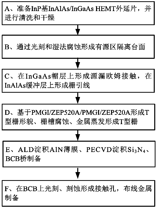
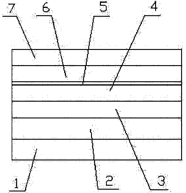
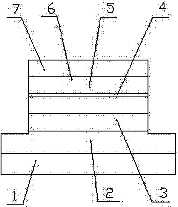
[0043] The cross-sectional structure of an anti-proton irradiation InP-based HEMT device based on aluminum nitride / silicon nitride stacked structure and BCB bridge is as follows: figure 1 shown. Its epitaxial structure from bottom to top is 100 μm thick InP substrate (InP Substrate), 500 nm thick InAlAs buffer layer (InAlAs Buffer), 15 nm thick InGaAs channel layer (InGaAs Channel), 3 nm thick InAlAs spacer (InAlAs Spacer), the doping concentration is 5×10 12 cm -2 Si surface doping layer (Si-Doping), 12nm thick InAlAs Schottky barrier layer (InAlAs Barrier), 30nm thick and doping concentration of 3×10 9 cm -2 InGaAs cap layer (InGaAs Cap); all InAlAs layers and InGaAs layers are lattice-matched with the InP substrate, the source isolation mesa is set on the InAlAs buffer layer, and the two sides of the highly doped InGaAs cap layer are respectively set There is a source ohmic contact metal and a drain ohmic contact metal, a grid is arranged on the InAlAs barrier layer b...


PUM

PropertyMeasurementUnit
Thicknessaaaaaaaaaa
Thicknessaaaaaaaaaa
Thicknessaaaaaaaaaa

Abstract

The invention belongs to the technical field of proton irradiation resistant semiconductor devices, and particularly relates to an anti-proton-irradiation InP-based HEMT device based on an aluminum nitride/silicon nitride stacked structure and a BCB bridge. The surface of the InP-based HEMT is covered with an AlN/Si3N4 stacked structure and a BCB bridge to serve as a passivation layer of the device, wherein the AlN/Si3N4 stacked structure can better inhibit the surface effect of the device; meanwhile, surface defects caused by plasma damage in the Si3N4 growth process of PECVD equipment are reduced; the BCB material has excellent nuclear resistance and electron resistance, the BCB bridge reduces parasitic distributed capacitance of the device and reduces internal heat accumulation of the device, proton irradiation resistance of the device is effectively improved, and influence on characteristics of the device is reduced.

Description

technical field [0001] The invention belongs to the technical field of anti-proton irradiation semiconductor devices, and in particular relates to an anti-proton irradiation InP-based HEMT device based on an aluminum nitride / silicon nitride stack structure and a BCB bridge. Background technique [0002] With people's pursuit of high-speed data communication and high-precision detection, the operating frequency of core integrated circuits is showing a trend of high frequency, gradually moving towards the terahertz field. InP-based HEMTs have the characteristics of high frequency, low noise, low power consumption and high gain. According to reports, the maximum oscillation frequency of the device ( f max ) exceeds 1.5 THz, the maximum current gain cutoff frequency ( f T ) over 700GHz. The operating frequency of InP-based HEMT integrated circuits has reached the millimeter wave range, and even reached the submillimeter wave range, showing great potential for military and c...

Claims


Application Information

Patent Timeline
IPC IPC(8): H01L29/778H01L23/29H01L23/552H01L21/335G03F7/00
CPCH01L29/7786H01L23/291H01L23/552H01L29/66462G03F7/00Y02P70/50
Inventor 钟英辉张佳佳靳雅楠赵向前孟圣皓
Owner ZHENGZHOU UNIV
Why Eureka
Try Eureka