

A paste based on multi-dimensional metal nanomaterials and its interconnection process
A metal nano and two-dimensional nano technology, applied in the fields of nanotechnology, nanotechnology, nanotechnology for materials and surface science, to achieve the effect of regulating mildness, improving shear strength, and realizing low-temperature sintering interconnection
- Summary
- Abstract
- Description
- Claims
- Application Information
AI Technical Summary
Problems solved by technology
Method used
Image

Examples
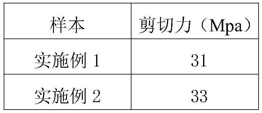
Embodiment 1
[0032] In a preferred embodiment of the present invention 1, the following steps are adopted to realize packaging and interconnection process:
[0033] 1. Preparation of multi-dimensional metal nano-interconnection materials
[0034] Use dry etching to form a number of holes with a diameter of 10nm on the surface of nano-silver wires and nano-silver sheets. Add nano-silver particles, etched nano-silver wires, etched nano-silver sheets, and hexanoic acid to the ethylene glycol solvent. 1. Phenolic resin, the mass ratio of which is 0.5:1:0.05:0.1, wherein the solid content of metal nanomaterials is about 80%, kept stirring at a constant speed for 300min, and concentrated by low-pressure rotary evaporation to obtain a uniformly dispersed paste.
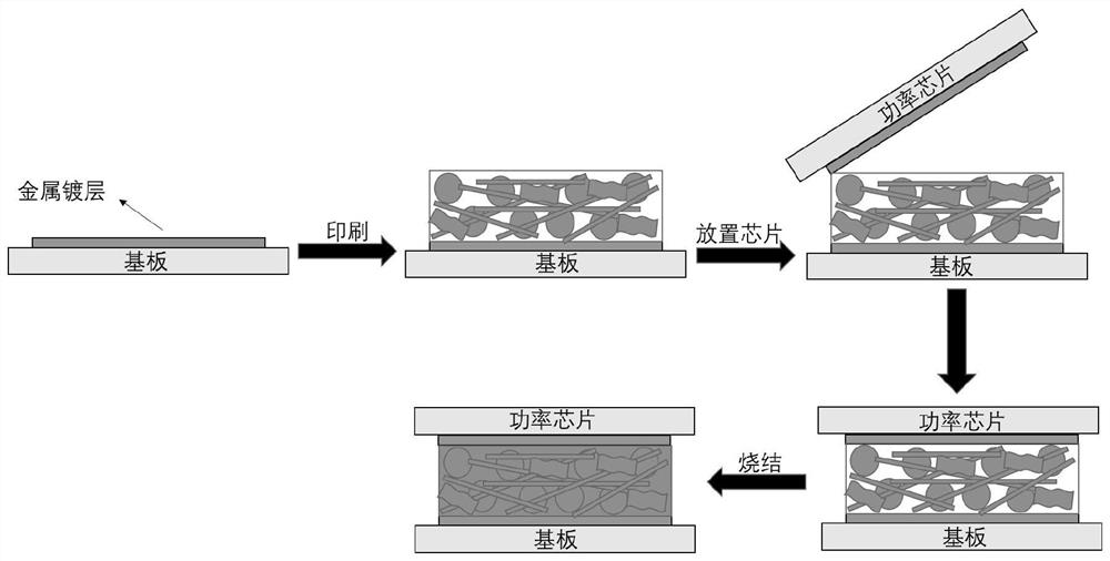
[0035] 2. Fabrication of Interconnect Devices
[0036] Print the above paste interconnect material on the copper-plated substrate by screen printing, slowly cover the copper-plated chip on the surface of the interconnect paste, place th...
Embodiment 2
[0038] In a preferred embodiment of the present invention 2, the following steps are adopted to realize the package interconnection process:
[0039] 1. Preparation of multi-dimensional metal nano-interconnection materials
[0040] Use dry etching to form a number of holes with a diameter of 40nm on the surface of nano-silver wires and nano-silver sheets. Add nano-silver particles, etched nano-silver wires, etched nano-silver sheets, and hexanoic acid to the ethylene glycol solvent. 1. Phenolic resin, the mass ratio of which is 0.5:1:0.05:0.1, wherein the solid content of metal nanomaterials is about 80%, kept stirring at a constant speed for 300min and concentrated by low-pressure rotary evaporation to obtain a uniformly dispersed paste.
[0041] 2. Fabrication of Interconnect Devices
[0042] Print the above paste interconnection material on the copper-plated substrate by screen printing, slowly cover the copper-plated chip on the surface of the interconnection paste, sinte...
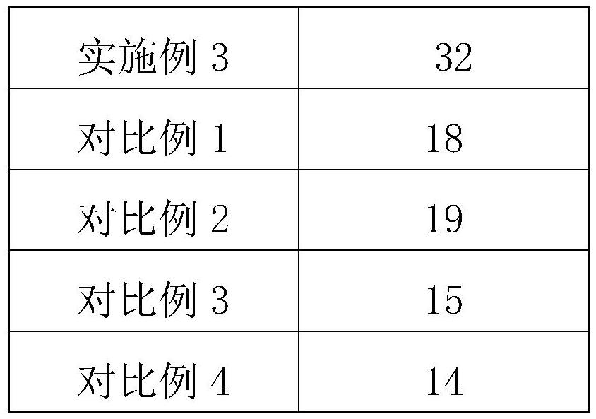
Embodiment 3
[0044] In a preferred embodiment of the present invention 3, the following steps are adopted to realize the package interconnection process:
[0045] 1. Preparation of multi-dimensional metal nano-interconnection materials
[0046] Use dry etching to form a number of holes with a diameter of 10nm on the surface of nano-silver wires and nano-copper sheets. Add nano-copper particles, etched nano-silver wires, etched nano-copper sheets, and o-phthalic acid to the ethylene glycol solvent. Diacid and polyvinyl butyral resin, the mass ratio of which is 0.2:0.8:0.01:0.05, ultrasonically oscillated for 60 minutes and concentrated by low-pressure rotary evaporation to obtain a uniformly dispersed paste, wherein the solid content of metal nanomaterials is 80%.
[0047] 2. Fabrication of Interconnect Devices
[0048] The above paste interconnect material was printed on the copper-plated substrate by screen printing, the copper-plated chip was slowly covered on the surface of the interco...
PUM
| Property | Measurement | Unit |
|---|---|---|
| diameter | aaaaa | aaaaa |
| particle diameter | aaaaa | aaaaa |
| length | aaaaa | aaaaa |
Abstract
Description
Claims
Application Information