Wafer with edge stepped/gentle slope type protection ring and manufacturing method thereof

A manufacturing method and technology of guard ring, which are applied in semiconductor/solid-state device manufacturing, electrical components, circuits, etc., can solve the problem of inability to apply simultaneous metal deposition process on both sides of thin wafers, and inability to perform photoresist spin coating process in yellow light process , the problem of inability to apply the proximity yellow light process, etc., to reduce the transfer steps, save the process time, and improve the yield.

Inactive Publication Date: 2020-07-24
绍兴同芯成集成电路有限公司
View PDF6 Cites 4 Cited by
  • Summary
  • Abstract
  • Description
  • Claims
  • Application Information

AI Technical Summary

Problems solved by technology

[0002] Wafer refers to the silicon wafer used in the production of silicon semiconductor integrated circuits. Because of its circular shape, it is called a wafer. It can be processed into various circuit element structures on the silicon wafer and become an IC with specific electrical functions. The product, the raw material of the wafer is silicon, and the silicon dioxide ore is refined by an electric arc furnace, chlorinated with hydrochloric acid, and distilled to produce high-purity polysilicon. After the wafer is thinned, many post-processing processes are required. To move a wafer thinned to 50-100 microns, one current method is to mechanically grind the wafer to generate a wafer with a thickness of 50-200 microns at the bottom of the wafer, leaving a 3-8 mm border ring, and then dry / wet etch The backside is treated by etching to improve the stress and poor roughness caused by mechanical grinding, and then the subsequent wafer production process begins. The circular structure generated by mechanical grinding has an almost 90-degree angle between the bottom of the wafer and the frame ring. structure, although it can meet the requirements of some subsequent production processes of thin wafers, it has the following disadvantages: the photoresist spin coating process of the yellow light process cannot be performed, because of its angular structure, the coated photoresist will be blocked by the edge Sputtering fails, and the proximity yellow light process cannot be applied. Because the proximity yellow light process requires the mask to be very close to the wafer, but it is blocked by the frame ring, and the process cannot be performed in a general and simple way, so it cannot Applying the double-sided simultaneous metal deposition process of thin wafers, in view of this situation, a method for manufacturing wafer edge step protection edge is proposed

Method used


Image

  • Wafer with edge stepped/gentle slope type protection ring and manufacturing method thereof
  • Wafer with edge stepped/gentle slope type protection ring and manufacturing method thereof
  • Wafer with edge stepped/gentle slope type protection ring and manufacturing method thereof

Examples


Embodiment 1

[0031] A method for manufacturing a wafer with an edge-stepped / gentle-slope guard ring, comprising the following steps:

[0032] Step 1: Paste the grinding film on the front of the wafer;

[0033] Step 2: Grind the back of the wafer, grind the thickness of the back of the ground wafer to 150-400 microns, lift and remove the grinding film;

[0034] Step 3: Use etching equipment, configure automatic thickness measurement, etchant concentration and flow control by etching process, and blocker is automatically controlled by the program to scale and protect the edge blocking ring / edge configuration with inert fluid nozzle dilution to reduce the amount of edge etching;

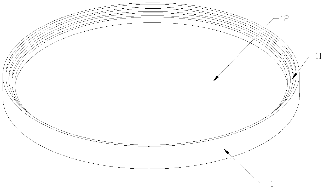
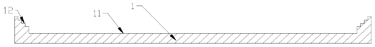
[0035] Step 4: Etching the back of the wafer to generate a protective ring with a width of 3-10 mm;

[0036] Step 5: Etching step by step, so that the height of the protection ring is gradually reduced from the outside to the inside, the protection ring is formed into a ladder shape, and the thickness of the wafer ...

Embodiment 2

[0038] A method for manufacturing a wafer with an edge-stepped / gentle-slope guard ring, comprising the following steps:

[0039] Step 1: Paste the grinding film on the front of the wafer;

[0040] Step 2: Grind the back of the wafer, grind the thickness of the back of the ground wafer to 150-400 microns, lift and remove the grinding film;

[0041] Step 3: Use etching equipment, configure automatic thickness measurement, etchant concentration and flow control by etching process, and blocker is automatically controlled by the program to scale and protect the edge blocking ring / edge configuration with inert fluid nozzle dilution to reduce the amount of edge etching;

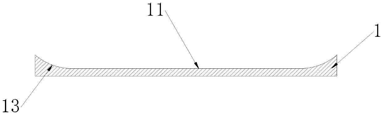
[0042] Step 4: Etching the back of the wafer to generate a protective ring with a width of 3-10 mm;

[0043] Step 5: Etching step by step, so that the height of the protection ring is gradually reduced from the outside to the inside, the protection ring forms a gentle slope shape, and the thickness of the wafer ins...


PUM

PropertyMeasurementUnit
thicknessaaaaaaaaaa

Abstract

The invention discloses a wafer with an edge stepped / gentle slope type protection ring and a manufacturing method of the wafer. The wafer with the edge stepped protection ring comprises a wafer body,and the wafer body is provided with a grinding front surface. The periphery of the wafer body is provided with a step protection ring / slope protection ring. The preparation method comprises the stepsof pasting a grinding pasting film on the front surface of the wafer; and grinding the back surface of the wafer, using etching equipment, automatically measuring the configuration thickness by an etching process, controlling the concentration and flow of etching liquid, automatically controlling the scaling of a blocking agent by a program to protect the edge shielding ring / edge configuration inert fluid nozzle to dilute and reduce the edge etching amount, etching the back surface of the wafer, and gradually reducing the height of the protection ring from outside to inside. The ultrathin wafer structure with the protection ring is used for subsequent ion implantation, yellow light and double-sided simultaneous metal deposition processes. The front side and back side processes can be carried out at the same time in one time of production, so that the process time is saved. The ultrathin wafer structure with the protection ring reduces the lost area of an edge wafer.

Description

technical field [0001] The invention relates to the field of semiconductors, in particular to a wafer with an edge stepped / gentle slope protection ring and a manufacturing method thereof. Background technique [0002] Wafer refers to the silicon wafer used in the production of silicon semiconductor integrated circuits. Because of its circular shape, it is called a wafer. It can be processed into various circuit element structures on the silicon wafer and become an IC with specific electrical functions. The product, the raw material of the wafer is silicon, and the silicon dioxide ore is refined by an electric arc furnace, chlorinated with hydrochloric acid, and distilled to produce high-purity polysilicon. After the wafer is thinned, many post-processing processes are required. To move a wafer thinned to 50-100 microns, one current method is to mechanically grind the wafer to generate a wafer with a thickness of 50-200 microns at the bottom of the wafer, leaving a 3-8 mm bor...

Claims


Application Information

Patent Timeline
Patent Type & Authority Applications(China)
IPC IPC(8): H01L21/304H01L21/306H01L29/06
CPCH01L21/304H01L21/30608H01L29/0684
Inventor 严立巍李景贤陈政勋
Owner 绍兴同芯成集成电路有限公司
Why Eureka
Try Eureka