Solar cell and laser slicing method
A solar cell and laser cutting technology, applied in laser welding equipment, circuits, photovoltaic power generation, etc., can solve the problems of solar cell efficiency loss, efficiency reduction, cell string welding mismatch, etc., to reduce the fill factor drop, weaken the Loss of efficiency, effect of eliminating damage
- Summary
- Abstract
- Description
- Claims
- Application Information
AI Technical Summary
Problems solved by technology
Method used
Image
Examples
Embodiment 1
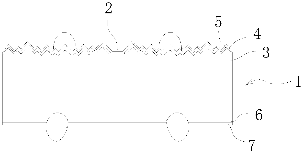
[0026] Such as figure 1 As shown, a solar cell includes a cell body 1 , and at least one emitter-free region 2 is provided on the front surface of the cell body 1 .
[0027] Specifically, the battery body 1 includes a p-type silicon substrate 3, the front surface of the p-type silicon substrate is sequentially provided with a PERC phosphorus diffused emitter 4 and a PERC battery anti-reflection film 5, and the rear surface of the p-type silicon substrate is The first PERC cell rear passivation layer 6 and the second PERC cell rear passivation layer 7 are arranged in sequence from the inside to the outside, and the emitter-free region 2 penetrates the PERC phosphorus diffused emitter 4 and the PERC cell anti-reflection film 5 .
[0028] In this embodiment, the emitter-free region 2 is rectangular, and separates the PERC phosphorus diffused emitter 4 and the PERC cell anti-reflection film 5 . The partition here refers to dividing the PERC phosphorus diffusion emitter 4 and the ...
Embodiment 2
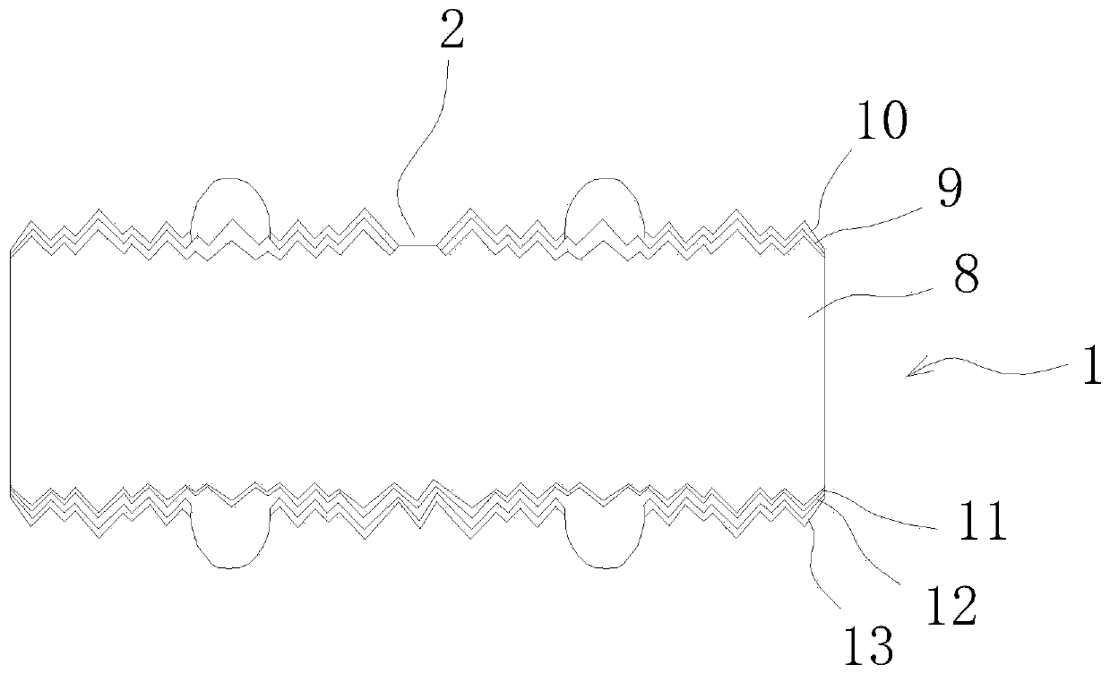
[0033] Such as figure 2 As shown, a solar cell includes a cell body 1 , and at least one emitter-free region 2 is provided on the front surface of the cell body 1 .
[0034] The battery body 1 includes an n-type silicon substrate 8, the front surface of the n-type silicon substrate 8 is provided with a TOPCon boron diffused emitter 9 and a TOPCon solar cell anti-reflection film 10 from the inside to the outside, and the rear surface of the n-type silicon substrate 8 is arranged from the inside to the outside A tunnel oxide layer 11 , a phosphorus-doped polysilicon film 12 and a SiNx:H film 13 on the back are provided in sequence, and the non-emitter region 2 penetrates the TOPCon boron diffused emitter 9 and the TOPCon solar cell anti-reflection film 10 .
[0035] The emitter-free region 2 is rectangular, and separates the TOPCon boron diffused emitter 9 and the TOPCon solar cell anti-reflection film 10 .
[0036] The emitter-free region 2 can be formulated according to the ...
Embodiment 3
[0040] combine figure 1 with figure 2As shown, the p-n junction side of the battery body 1 is provided with a laser, and the phosphosilicate glass or borosilicate glass on the p-n surface is scratched at the subsequent laser slicing position, and then wet-etched, dry-etched or mechanically etched The p-n structure in the film-opening area is removed to form an emitter-free area 2, and a battery is made, and then a laser is used to cut along the emitter-free area 2 to split the battery body 1. The width of the emitter-free region 2 is 40 μm-2000 μm, the depth is less than 1 μm, and the spot size of the laser cutting line along the emitter-free region 2 is 5-50 μm. The laser cutting line is located within ±200 μm of the central axis of the emitter-free region 2 . Preferably, the central axis of the laser cutting line coincides with the central axis of the emitter-free region 2 .
[0041] In this embodiment, a low-power film-opening laser is used to cut the phosphosilicate gl...
PUM
| Property | Measurement | Unit |
|---|---|---|
| Width | aaaaa | aaaaa |
| Depth | aaaaa | aaaaa |
| Depth | aaaaa | aaaaa |
Abstract
Description
Claims
Application Information

