A self-aligned in-situ characterization chip and its preparation and use method

A self-aligning, in-situ technology, applied in material analysis using radiation, material analysis using radiation diffraction, and material analysis using wave/particle radiation, etc., can solve problems such as hindering sample observation, and achieve easy learning and The effect of promotion, simple use method and good material compatibility

Active Publication Date: 2021-10-22
SHANGHAI INST OF MICROSYSTEM & INFORMATION TECH CHINESE ACAD OF SCI
View PDF0 Cites 0 Cited by
  • Summary
  • Abstract
  • Description
  • Claims
  • Application Information

AI Technical Summary

Problems solved by technology

Damage and contamination introduced by this process can hinder sample observation

Method used


Image

  • A self-aligned in-situ characterization chip and its preparation and use method
  • A self-aligned in-situ characterization chip and its preparation and use method
  • A self-aligned in-situ characterization chip and its preparation and use method

Examples


no. 1 example

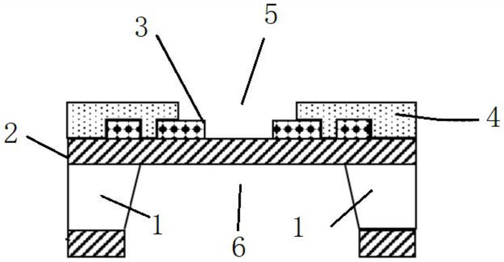
[0038] The first embodiment A self-aligned in-situ characterization chip for background observation

[0039] Such as figure 1 Shown is a self-aligned in-situ characterization chip according to the first embodiment of the present invention, which is used for in-situ observation of a sample to be tested, including a substrate layer 1, the front and back of the substrate layer 1 A first insulating layer 2 and a second insulating layer 2' are provided respectively. Wherein, the substrate layer 1 is used to support structures such as the first insulating layer 2 and the second insulating layer 2', and the material of the substrate layer 1 is silicon, silicon carbide or gallium nitride. In this embodiment, the substrate layer 1 is a circular silicon wafer with a thickness of 400-500 μm.

[0040] The first insulating layer 2 has a front side away from the substrate layer 1, a functional layer 3 and a third insulating layer 4 are arranged on the front side of the first insulating la...

no. 2 example

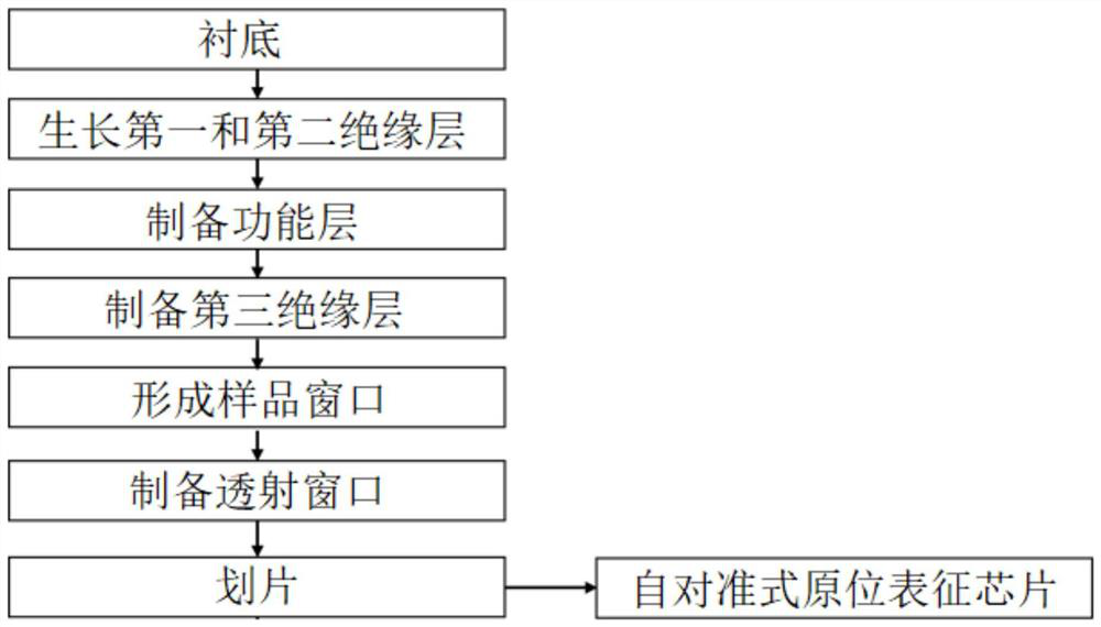
[0043] Second embodiment A method for preparing a self-aligned in-situ characterization chip

[0044] Such as figure 2 Shown is a method for preparing a self-aligned in-situ characterization chip according to the second embodiment of the present invention, which is used to prepare the self-aligned in-situ characterization chip according to the first embodiment of the present invention.

[0045] Such as figure 2 As shown, in this embodiment, the preparation method of the self-aligned in-situ characterization chip comprises the following steps:

[0046] Step S1: preparing a substrate sheet, growing a first insulating layer 2 and a second insulating layer 2' on the front and back sides of the substrate sheet respectively;

[0047] Wherein, the first insulating layer 2 is deposited and grown on the surface of the substrate by low pressure chemical vapor deposition (LPCVD), plasma enhanced chemical vapor deposition or atomic layer deposition. The substrate is a 4-inch Si (100)...

no. 3 example

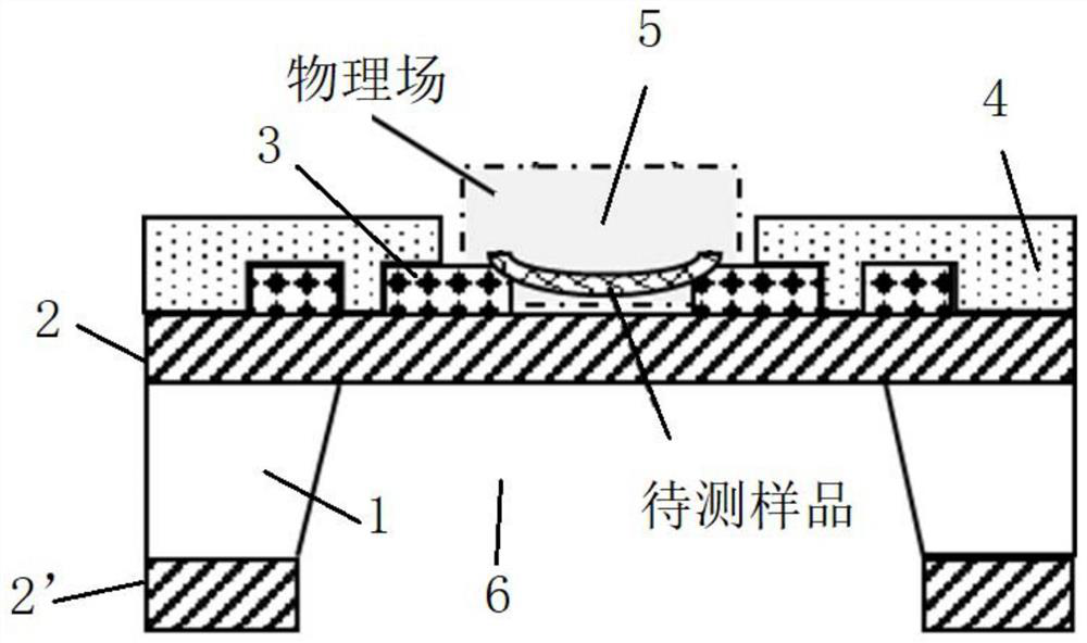
[0071] The third embodiment A method of using a self-aligned in-situ characterization chip

[0072] According to the third embodiment of the present invention, the self-aligned in-situ characterization chip used in the method for using the self-aligned in-situ characterization chip is the same as the above-mentioned self-aligned in-situ characterization chip according to the first embodiment of the present invention. The quasi-type in-situ characterization chip is exactly the same, and this method is used for in-situ observation of a sample to be tested by a transmission electron microscope (TEM).

[0073] Such as image 3 As shown, the method for using the self-aligned in-situ characterization chip specifically includes the following steps:

[0074] Step S1': providing a self-aligned in-situ characterization chip according to the first embodiment of the present invention;

[0075] Step S2': Prepare a sample to be tested in the sample window 5 of the self-aligned in-situ cha...


PUM

PropertyMeasurementUnit
thicknessaaaaaaaaaa
thicknessaaaaaaaaaa
diameteraaaaaaaaaa

Abstract

The present invention provides a self-aligned in-situ characterization chip, which includes a substrate layer, first and second insulating layers are provided on the front and back of the substrate layer, and a part of the first insulating layer is provided on the front of the first insulating layer. A functional layer and a third insulating layer covering a part of the exposed part of the first insulating layer and a part of the functional layer; a part of the first insulating layer is exposed on the third insulating layer and the functional layer, and a part of the functional layer is exposed on the first insulating layer Three insulating layers to form a sample window; the second insulating layer is provided with a transmission window aligned with the sample window. The invention also provides methods for their preparation and use. The characterization chip allows the sample to be tested to be self-aligned and connected to the functional layer through the sample window, thereby avoiding the operation of sample preparation and transferring the sample to the characterization chip, and eliminating the possibility of sample contamination and damage during the corresponding process.

Description

technical field [0001] The invention relates to the field of in-situ electron microscopy characterization, in particular to a self-aligned in-situ characterization chip and a preparation and use method thereof. Background technique [0002] Advanced characterization methods are an important driving force for the progress of materials science. Transmission electron microscopy (TEM, referred to as TEM) is one of the important means to study the microstructure of materials. In addition to static observation of the sample, people also hope to introduce external physical fields such as force, electricity, heat, light, gas, liquid, etc., to observe the microstructure and physical property changes of the material under the action of the external field in situ, that is, the dynamic observation of the sample. [0003] At present, the dynamic observation can be mainly completed through the environmental transmission electron microscope or the transmission electron microscope sample r...

Claims


Application Information

Patent Timeline
Patent Type & Authority Patents(China)
IPC IPC(8): G01N23/2005G01N23/20025G01N23/04G01N23/20
CPCG01N23/04G01N23/20G01N23/20025G01N23/2005
Inventor 刘梦王跃林李铁
Owner SHANGHAI INST OF MICROSYSTEM & INFORMATION TECH CHINESE ACAD OF SCI
Why Eureka
Try Eureka