Manufacturing method of electromagnetic shielding material, electromagnetic shielding material and electronic product

A technology of electromagnetic shielding material and manufacturing method, which is applied in the fields of magnetic field/electric field shielding, metal material coating process, electrical components, etc., can solve the problem of long production process flow of conductive cloth, unsatisfactory adhesion of metal layer, and difficulty of accurate conductive cloth. Control and other issues to achieve the effect of improving the use effect and flexibility of use, good coating effect and low cost

Pending Publication Date: 2020-08-04
深圳市乐工新技术有限公司
View PDF4 Cites 0 Cited by
  • Summary
  • Abstract
  • Description
  • Claims
  • Application Information

AI Technical Summary

Problems solved by technology

However, the production process of the existing conductive cloth is long, after several chemical plating or electroplating processes, the environmental pollution is large, and the adhesion of the metal layer is not ideal.
Moreover, due to the requirements of the process, the thickness of the conductive cloth is difficult to make thin, and its thickness is usually more than 18 microns; in addition, due to the difficulty of precise control in the production process of the conductive cloth, the product qualification rate is low and the cost is high

Method used


Image

  • Manufacturing method of electromagnetic shielding material, electromagnetic shielding material and electronic product
  • Manufacturing method of electromagnetic shielding material, electromagnetic shielding material and electronic product
  • Manufacturing method of electromagnetic shielding material, electromagnetic shielding material and electronic product

Examples


Embodiment 1

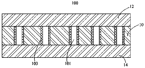
[0065] A polymer film layer is provided, the thickness of the polymer film layer is 1.5 microns, and the material is polyethylene terephthalate.

[0066] The polymer film layer is baked at a temperature of 45 degrees centigrade for 24 hours.

[0067] Laser drilling is performed on the baked polymer film layer to form a plurality of through holes in the polymer film layer, the diameter of the through holes is 0.1 micron, the hole distance is 0.1 micron, and the shape of the several through holes is circular.

[0068] Corona treatment was performed on both surfaces of the perforated polymer film layer, and the corona treatment time was 1 second. The dyne value of both surfaces after corona treatment was 56.

[0069] A layer of metal shielding layer is respectively sputtered on the two surfaces of the polymer film layer after corona treatment and the walls of several through holes, with copper as the target material, and continuous winding coating is adopted. The coating process...

Embodiment 2

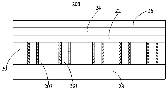
[0072] A polymer film layer is provided, the thickness of the polymer film layer is 6 microns, and the material is polycarbonate.

[0073] The polymer film layer is baked at a temperature of 80 degrees centigrade for 1 hour.

[0074] Laser drilling is performed on the baked polymer film layer to form a plurality of through holes in the polymer film layer, the diameter of the through holes is 100 microns, and the hole distance is 100 microns. The shapes of the through holes are triangles.

[0075] Corona treatment was performed on the two surfaces of the perforated polymer film layer, and the corona treatment time was 10 seconds respectively. The dyne value of both surfaces after corona treatment was 54.

[0076] The first layer of metal shielding layer is sputtered on the two surfaces of the polymer film layer after corona treatment and the hole walls of several through holes, with zinc as the target material, and continuous winding coating is adopted. The coating process co...

Embodiment 3

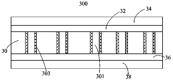
[0079] A polymer film layer is provided, the thickness of the polymer film layer is 2 microns, and the material is polypropylene.

[0080] Laser drilling is performed on the polymer film layer to form a plurality of through holes in the polymer film layer. The diameter of the through holes is 10 microns, the distance between the holes is 10 microns, and the shape of the several through holes is quadrilateral.

[0081] The two surfaces of the polymer film layer were subjected to corona treatment, and the corona treatment time was 5 seconds respectively. The dyne values ​​of the two surfaces after corona treatment were 40 respectively.

[0082] A metal shielding layer is respectively sputtered on the two surfaces of the corona-treated polymer film layer and the walls of several through holes, with titanium as the target material, and continuous winding coating is adopted. The coating process conditions are: vacuum The temperature is 0.2Pa, the continuous winding plating speed i...


PUM

PropertyMeasurementUnit
thicknessaaaaaaaaaa
thicknessaaaaaaaaaa
pore sizeaaaaaaaaaa

Abstract

The invention discloses a manufacturing method of an electromagnetic shielding material, the electromagnetic shielding material prepared by the manufacturing method and an electronic product applyingthe electromagnetic shielding material. The manufacturing method of the electromagnetic shielding material comprises the following steps: providing a polymer film layer of which two sides are conducted, wherein the thickness of the polymer film layer is greater than or equal to 0.8 micron and less than or equal to 12 microns; roughening the polymer film layer to enable the dyne value of the polymer film layer to be greater than or equal to 44 and less than or equal to 70; performing vapor deposition on the two roughened surfaces, forming at least one metal shielding layer on each surface, andperforming the metal shielding layers on the two surfaces through the polymer film layer; according to the technical scheme, the electromagnetic shielding material which is very thin and is conductedon two sides is provided.

Description

technical field [0001] The invention relates to the technical field of electromagnetic shielding, in particular to a manufacturing method of an electromagnetic shielding material, an electromagnetic shielding material prepared by the method, and an electronic product using the electromagnetic shielding material. Background technique [0002] Conductive cloth is an electromagnetic shielding material with good conductivity and electromagnetic wave shielding effect. Electromagnetic shielding conductive cloth is widely used in electronics, instrumentation and other industries due to its excellent vertical conduction and shielding performance, and can prevent damage and aging of electronic components caused by static electricity. However, the production process of the existing conductive cloth is long, and after several chemical plating or electroplating processes, the environmental pollution is large, and the adhesion of the metal layer is not ideal. Moreover, due to the requir...

Claims


Application Information

Patent Timeline
Patent Type & Authority Applications(China)
IPC IPC(8): C08J7/06C08J7/12C08L67/02C08L69/00C08L23/12C08L23/20C08L79/08C23C14/20C23C14/34H05K9/00
CPCC08J7/06C08J7/123C23C14/34C23C14/205H05K9/0081C08J2367/02C08J2369/00C08J2323/12C08J2323/20C08J2379/08
Inventor 夏祥国李林军任诗举
Owner 深圳市乐工新技术有限公司
Why Eureka
Try Eureka