A chip package electrode and its preparation method and chip package structure

A chip packaging structure, chip packaging technology, applied in the direction of circuits, electrical components, electrical solid devices, etc., can solve the problems of high risk of mechanical damage, poor heat dissipation of chips, etc., to reduce the risk of mechanical damage, reduce damage, and increase electrical conductivity Effect

Active Publication Date: 2021-09-21
GLOBAL ENERGY INTERCONNECTION RES INST CO LTD
View PDF1 Cites 0 Cited by
  • Summary
  • Abstract
  • Description
  • Claims
  • Application Information

AI Technical Summary

Problems solved by technology

[0005] Therefore, the technical problem to be solved by the present invention is to overcome the defects of high risk of mechanical damage in the rigid crimping chip packaging structure and poor heat dissipation of the chip in the elastic crimping chip packaging structure in the prior art, thereby providing a chip packaging electrode and its Fabrication method and chip packaging structure

Method used


Image

  • A chip package electrode and its preparation method and chip package structure
  • A chip package electrode and its preparation method and chip package structure
  • A chip package electrode and its preparation method and chip package structure

Examples


preparation example Construction

[0070] Preparation method of chip package electrode

[0071] The present invention also provides a method for preparing the chip packaging electrode, comprising:

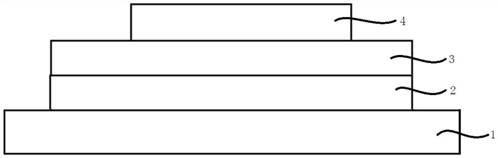
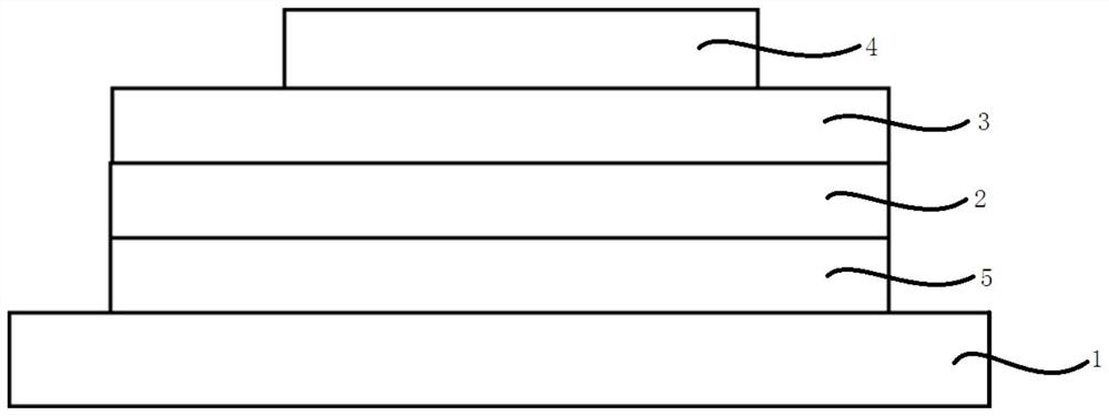
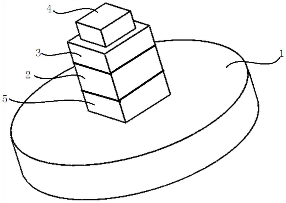
[0072] A first molybdenum-copper alloy layer 2 , an elastic layer 3 and a second molybdenum-copper alloy layer 4 are sequentially formed on the electrode plate 1 .

[0073] All conventional preparation methods capable of forming the above chip package electrode structure are within the protection scope of the present invention.

Embodiment approach

[0074] As an optional embodiment of the preparation method, the preparation is carried out according to the following steps:

[0075] The first molybdenum-copper alloy layer, the elastic layer and the second molybdenum-copper alloy layer are sequentially formed on the electrode plate by 3D printing technology to obtain alloy formed parts;

[0076] The alloy formed part is heat-treated to obtain the chip packaging electrode.

[0077] The application of 3D printing technology is conducive to the flexible adjustment of molybdenum and copper content in the first molybdenum-copper alloy layer and the second molybdenum-copper alloy layer, and is conducive to the uniform distribution of copper and elastomer in the elastic layer.

[0078] The specific operation method is given below:

[0079] (1) Lay copper powder on the electrode plate, heat the copper powder in the selected area with a laser beam, fuse the copper powder in the selected area, form a laser cladding layer on the surfa...

Embodiment 1

[0105] This embodiment provides a chip packaging electrode, the preparation method of which is as follows:

[0106] (1) Lay copper powder on the copper plate, heat the copper powder in the selected area with a laser beam, fuse the copper powder in the selected area, form a laser cladding layer on the surface of the copper plate, print to a predetermined height, and obtain a copper metal layer , the thickness is 10mm, the particle size of copper powder is 15-60μm, and the oxygen content is lower than 2000ppm;

[0107] (2) Lay the mixed powder of molybdenum and copper on the copper metal layer obtained in step (1), heat the mixed powder of molybdenum and copper in the selected area with a laser beam, and fuse the mixed powder of molybdenum and copper in the selected area , a laser cladding layer is formed on the surface of the copper metal layer. As the printing height increases, the mass percentage of molybdenum in the mixed powder of molybdenum and copper increases from 0% to ...


PUM

PropertyMeasurementUnit
thicknessaaaaaaaaaa
particle diameteraaaaaaaaaa
thicknessaaaaaaaaaa

Abstract

The invention provides a chip packaging electrode, a preparation method thereof and a chip packaging structure. The chip packaging electrode includes: an electrode plate and a first molybdenum-copper alloy layer, an elastic layer and a second molybdenum-copper alloy layer stacked on the electrode plate, wherein the first molybdenum-copper alloy layer and the second molybdenum-copper alloy layer The mass percentage of molybdenum in the copper alloy layer increases gradually along the direction away from the electrode plate, and the elastic layer is made of a composite material formed of copper and elastomer. In the first molybdenum-copper alloy layer and the second molybdenum-copper alloy layer, copper ensures that the electrode has excellent electrical conductivity. Since the thermal expansion coefficient of molybdenum is more compatible with the chip, the damage caused by the thermal expansion coefficient mismatch to the electrode or chip is reduced. ; In the elastic layer, copper ensures the conductivity of the electrode, and the addition of elastomer increases the elasticity of the electrode, further reducing the risk of mechanical damage to the chip. The packaging electrode has a compact structure, and the distance between the electrode and the chip is suitable, which ensures good heat dissipation of the chip.

Description

technical field [0001] The invention relates to the technical field of chip packaging, in particular to a chip packaging electrode, a preparation method thereof, and a chip packaging structure. Background technique [0002] At present, power semiconductor devices are developing rapidly. For example, thyristors and insulated gate bipolar transistors (IGBTs) are widely used in new energy, power transmission, rail transit, metallurgy, and chemical industries. Press-fit packaging is an important form of power semiconductor device packaging, especially widely used in IGBT chip packaging. In the press-fit packaging structure, the emitter and collector of the IGBT module are connected to the chip through pressure Package electrodes are connected. The press-connect IGBT module is very suitable for high-voltage and high-power applications such as power systems, electric locomotives, and smart grids due to its advantages of dense chip layout, double-sided heat dissipation, high power...

Claims


Application Information

Patent Timeline
Patent Type & Authority Patents(China)
IPC IPC(8): H01L23/047H01L21/48H01L23/367H01L23/373
CPCH01L21/4817H01L23/047H01L23/3677H01L23/3735
Inventor 王亮石浩吴军民金锐张朋唐新灵林仲康周扬
Owner GLOBAL ENERGY INTERCONNECTION RES INST CO LTD
Why Eureka
Try Eureka