Double-sided selective emitter high-efficiency crystalline silicon cell and preparation method thereof

A technology of crystalline silicon cells and emitters, applied in photovoltaic power generation, circuits, electrical components, etc., can solve the problems of inability to passivate boron doping, difficult implementation, and immature technology, so as to avoid light absorption, improve Isc, and improve Effect of Surface Doping Concentration

Active Publication Date: 2020-08-11
CHANGZHOU UNIV +1
View PDF7 Cites 18 Cited by
  • Summary
  • Abstract
  • Description
  • Claims
  • Application Information

AI Technical Summary

Problems solved by technology

However, the efficiency of the existing mass production process of n-TOPCon batteries has not widened the gap with PERC batteries, and the efficiency difference is only 0.5%. Therefore, how to improve the efficiency of batteries with this structure has become a top priority.
[0003] The conventional boron-doped selective emitter on the front side is difficult to realize by conventional etching and laser or APCVD, and the current technology is immature
However, the use of silicon oxide as the tunneling layer cannot passivate boron-doped
The conventional selective emitter on the back side is the existing technical solution of etching and laser, but the laser method cannot be used for phosphorus-doped polysilicon, because the laser will damage the tunnel oxide layer, and the simple etching solution is suitable for polysilicon with uniform doping concentration The structure is also infeasible

Method used


Image

  • Double-sided selective emitter high-efficiency crystalline silicon cell and preparation method thereof
  • Double-sided selective emitter high-efficiency crystalline silicon cell and preparation method thereof
  • Double-sided selective emitter high-efficiency crystalline silicon cell and preparation method thereof

Examples


Embodiment 1

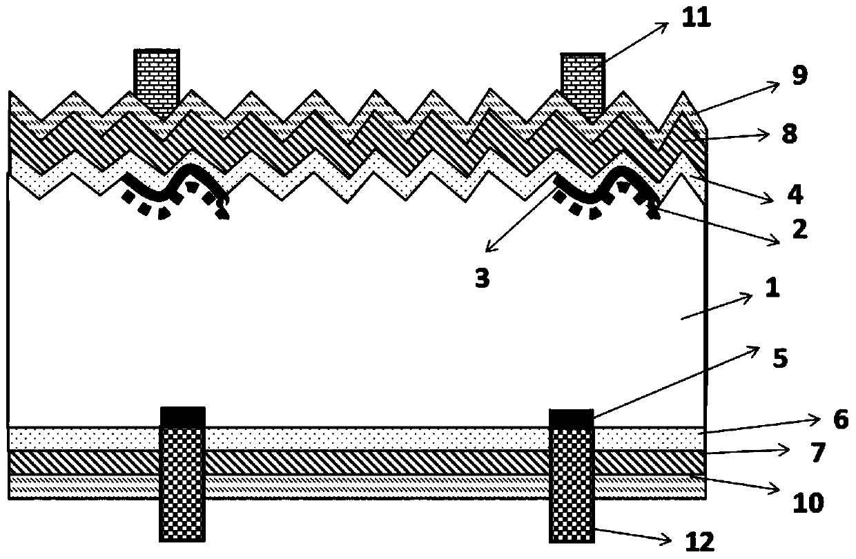
[0059] A double-sided selective emitter extremely high-efficiency crystalline silicon battery specific battery manufacturing steps are as follows:

[0060] An N-type silicon wafer with a high minority carrier lifetime is used as the substrate (1), its resistivity is 0.8Ω.cm, and the minority carrier lifetime is >1ms.

[0061] (1) Double-sided texturing, in the groove machine, first use KOH:H 2 o 2 =1:3 for pre-cleaning 2min, the temperature is maintained at 75 ° C; then in KOH: additive = 8: 1 (the additive is composed as follows according to the number of parts: 5 parts of sodium lactate, 8 parts of surfactant (wherein, sodium hydroxide: poly Ether modified polysiloxane defoamer=1:2 (mass ratio)), 1 part of methyl glucose polyoxyethylene ether; 2 parts of glucose; 1 part of polyacrylamide; 83 parts of deionized water), the temperature is maintained at 80 ℃, time 7min for rapid texturing; the amount of thinning is controlled at about 0.55g.

[0062] (2) Intrinsic polysilico...

Embodiment 2

[0076] A double-sided selective emitter extremely high-efficiency crystalline silicon battery specific battery manufacturing steps are as follows:

[0077] An N-type silicon wafer with a high minority carrier lifetime is used as the substrate (1), its resistivity is 1.5Ω.cm, and the minority carrier lifetime is >1.5ms.

[0078] (1) Double-sided velvet, pre-cleaned for 2 minutes in the tank machine, KOH:H 2 o 2 =1:4, the temperature is maintained at 80°C; then in KOH: additive=7:1 (the composition of the additive is as follows according to the number of parts: 6 parts of sodium lactate, 9 parts of surfactant (sodium hydroxide: polyether modified silicone Alkanes antifoaming agent=1:2.5 (mass ratio)), 1.5 parts of methyl glucose polyoxyethylene ether; 2 parts of glucose; 1.5 parts of polyacrylamide; 80 parts of deionized water), the temperature was maintained at 75 ° C, and the time was 7 minutes. Fast velvet. The amount of thinning is controlled at about 0.5g;

[0079] (2) ...


PUM

PropertyMeasurementUnit
thicknessaaaaaaaaaa
thicknessaaaaaaaaaa
thicknessaaaaaaaaaa

Abstract

The invention belongs to the field of solar photovoltaic industry and particularly provides a double-sided selective emitter efficient crystalline silicon cell and a preparation method thereof. The double-sided selective emitter efficient crystalline silicon cell is characterized in that a double-sided selective emitter structure is adopted, a boron-doped heavily-doped region is a polycrystallinesilicon structure in which aluminum oxide replaces silicon oxide to serve as a tunneling layer, a constant surface concentration increase fill factor (FF) exceeding 1E20atom/cm <3> can be achieved, alightly-expanded region is pure boron doping, a heavily-expanded boron doping process and a lightly-expanded boron doping process can be realized in one step, and the process is simplified. Silicon oxide is adopted as a tunneling layer for a phosphorus-doped region, a heavily-doped region is of a double-layer poly structure, the surface concentration is high, metallization contact is improved, a lightly-expanded region is of a single-layer lightly-doped poly structure, and then the open-circuit voltage (Voc) is increased. The formation of the double-sided selective emitter effectively utilizesa mask etching mode. The double-sided selective emitter efficient crystalline silicon cell is advantaged in that the structure can effectively improve battery efficiency, and is suitable for batch production.

Description

technical field [0001] The invention belongs to the field of solar crystal silicon cells, in particular to a double-sided selective emitter high-efficiency crystal silicon cell and a preparation method thereof. Background technique [0002] The pursuit of high-efficiency cells is a development trend in the photovoltaic industry. The solution that takes into account both cost and process is the n-TOPCon cell, which uses an ultra-thin oxide layer and doped thin-film silicon to passivate the back of the cell. Among them, the backside oxide layer has a thickness of 1.4nm and is grown by wet chemical method. Then on the oxide layer, 20nm phosphorous-doped amorphous silicon is deposited, and then annealed to recrystallize and strengthen the passivation effect. It will become the next-generation mainstream product after PERC. For the existing n-TOPCon battery mass production process, its efficiency has not widened the gap with PERC batteries, and the efficiency difference is only...

Claims


Application Information

Patent Timeline
Patent Type & Authority Applications(China)
IPC IPC(8): H01L31/0224H01L31/0216H01L31/0352H01L31/068H01L31/18
CPCH01L31/02167H01L31/022441H01L31/035272H01L31/0684H01L31/1804H01L31/186H01L31/1868Y02E10/547Y02P70/50
Inventor 袁宁一王芹芹丁建宁程广贵王书博
Owner CHANGZHOU UNIV
Why Eureka
Try Eureka