A kind of Schottky type perovskite photodetector and preparation method thereof

A photodetector and perovskite technology, applied in photovoltaic power generation, electrical solid-state devices, semiconductor/solid-state device manufacturing, etc.

Active Publication Date: 2022-05-20
HUAZHONG UNIV OF SCI & TECH
View PDF5 Cites 0 Cited by
  • Summary
  • Abstract
  • Description
  • Claims
  • Application Information

AI Technical Summary

Problems solved by technology

[0004] For the above defects or improvement needs of existing perovskite photodetectors, the object of the present invention is to provide a Schottky type perovskite photodetector and a preparation method thereof, the Schottky type perovskite photodetector It is constructed by using the metal-semiconductor rectifying contact characteristics, and has a good inhibitory effect on the dark current through the Schottky barrier; at the same time, by spin-coating a layer of polyimide PI film on the surface of the perovskite, using polyimide The passivation of the perovskite surface and the barrier reaction between the metal and the perovskite can reduce the dark current and ion migration of the perovskite photodetector by the amine PI thin film, thereby effectively suppressing the dark state of the perovskite photodetector when it is working. Excessive current and dark current drift issues

Method used


Image

  • A kind of Schottky type perovskite photodetector and preparation method thereof
  • A kind of Schottky type perovskite photodetector and preparation method thereof
  • A kind of Schottky type perovskite photodetector and preparation method thereof

Examples


Embodiment example 1

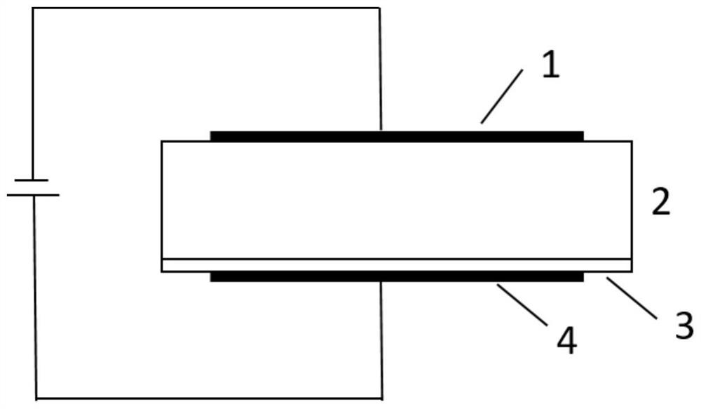
[0028] (1) Prepare a 15% PI (polyimide) solution, weigh 0.57 g of biphenyltetracarboxylic dianhydride and 0.2 g of p-phenylenediamine in turn, add them to 5 mL of N-methylpyrrolidone (NMP), and stir to dissolve .

[0029] (2) in cesium lead bromide (CsPbBr 3 ) spin-coating PI (polyimide) solution on perovskite single crystal, after spin-coating, cesium lead bromide (CsPbBr 3 ) The perovskite single crystal was placed on a hot stage and heated at 80 °C for 10 minutes to obtain a PI film with a thickness of 300 nm.

[0030] (3) A silver electrode was vapor-deposited on the PI (polyimide) film.

[0031] (4) in cesium lead bromide (CsPbBr 3 ) A gold electrode was evaporated on the other side of the perovskite single crystal.

Embodiment example 2

[0033] (1) Prepare a 5% PI (polyimide) solution, weigh 0.19 g of biphenyltetracarboxylic dianhydride and 0.07 g of p-phenylenediamine in turn, add them to 5 mL of N-methylpyrrolidone (NMP), and stir to dissolve .

[0034] (2) in cesium lead bromide (CsPbBr 3 ) spin-coated PI (polyimide) solution on perovskite multi-wafer, after spin-coating, cesium lead bromide (CsPbBr 3) The perovskite multi-wafer was placed on a hot stage and heated at 80 °C for 10 minutes to obtain a PI film with a thickness of 20 nm.

[0035] (3) A silver electrode was vapor-deposited on the PI (polyimide) film.

[0036] (4) in cesium lead bromide (CsPbBr 3 ) A gold electrode was evaporated on the other side of the perovskite polymorph.

Embodiment example 3

[0038] (1) Prepare a 15% PI (polyimide) solution, weigh 0.57 g of biphenyltetracarboxylic dianhydride and 0.2 g of p-phenylenediamine in turn, add them to 5 mL of dimethylformamide (DMF), and stir to dissolve .

[0039] (2) in cesium lead bromide (CsPbBr 3 ) spin-coating PI (polyimide) solution on perovskite single crystal, after spin-coating, cesium lead bromide (CsPbBr 3 ) The perovskite single crystal was placed on a hot stage and heated at 80 °C for 10 minutes to obtain a PI film with a thickness of 300 nm.

[0040] (3) A silver electrode was vapor-deposited on the PI (polyimide) film.

[0041] (4) in cesium lead bromide (CsPbBr 3 ) A gold electrode was evaporated on the other side of the perovskite single crystal.


PUM

PropertyMeasurementUnit
thicknessaaaaaaaaaa
electron work functionaaaaaaaaaa

Abstract

The invention belongs to the technical field of semiconductor photodetectors, and discloses a Schottky type perovskite photodetector and a preparation method thereof, wherein the Schottky type perovskite photodetector comprises first metal electrodes (1 ), a perovskite light-absorbing layer (2), a polyimide PI layer (3) and a second metal electrode (4), wherein the metal material used in the first metal electrode (1) has a higher work function, The metal material used for the second metal electrode (4) has a lower work function. The invention has a good inhibitory effect on dark current through the Schottky potential barrier; meanwhile, by spin-coating a layer of polyimide (PI) film on the surface of the perovskite, the polyimide (PI) film is used for The passivation of the perovskite surface and the reaction between the blocking metal and the perovskite can reduce the dark current and ion migration of the perovskite photodetector, thereby effectively suppressing the excessive dark current and dark current of the perovskite photodetector during operation. Drift problem.

Description

technical field [0001] The invention belongs to the technical field of semiconductor photodetectors, and more particularly relates to a Schottky type perovskite photodetector and a preparation method thereof. Background technique [0002] A photodetector is a device that captures light signals in a specific wavelength range and instantly converts them into electrical signals. Photodetectors have important and extensive applications in the fields of optical imaging, optical communication, automatic control, and biochemical sensing. Therefore, it is of great significance to develop photodetectors with superior performance. Semiconductor photodetectors can be divided into photoconductive detectors, photodiodes and phototriodes. Currently, photodetectors based on semiconductor materials such as silicon, germanium, indium, gallium arsenide, and gallium nitride are widely used in commercial products to cover different spectral ranges due to their different band gaps. [0003] C...

Claims


Application Information

Patent Timeline
Patent Type & Authority Patents(China)
IPC IPC(8): H01L51/42H01L51/44H01L51/46H01L51/48
CPCH10K71/00H10K30/10H10K30/80H10K30/88Y02E10/549
Inventor 牛广达杜鑫源唐江逄锦聪潘伟程朱劲松
Owner HUAZHONG UNIV OF SCI & TECH
Why Eureka
Try Eureka