Nonplanar patterned nanostructured surface and printing methods for making thereof
A non-planar, patterned technology, applied in the field of layout of patterned elements, can solve problems such as long patterning time, limited size and pattern geometry, excessive feature structure, etc.
- Summary
- Abstract
- Description
- Claims
- Application Information
AI Technical Summary
Problems solved by technology
Method used
Image

Examples
Embodiment 1
[0089] A silver-plated PET film was wrapped on the surface of the cylindrical roll. A PDMS stamp having dimensions of about 2 cm x 3 cm was impregnated with a solution of 10 mM thiol in ethanol, and the solution was allowed to penetrate into the stamp for about 30 minutes to 10 hours.
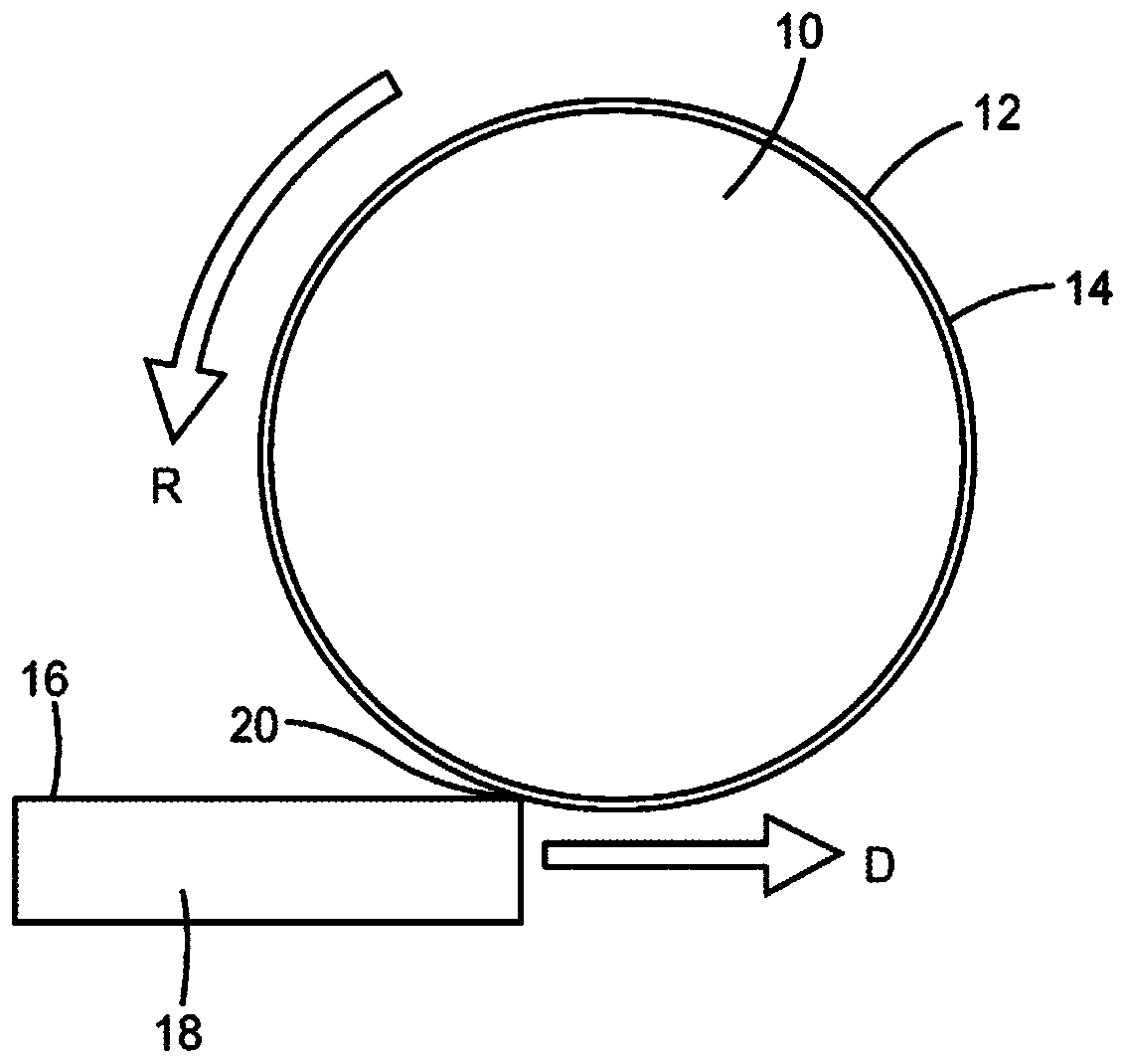
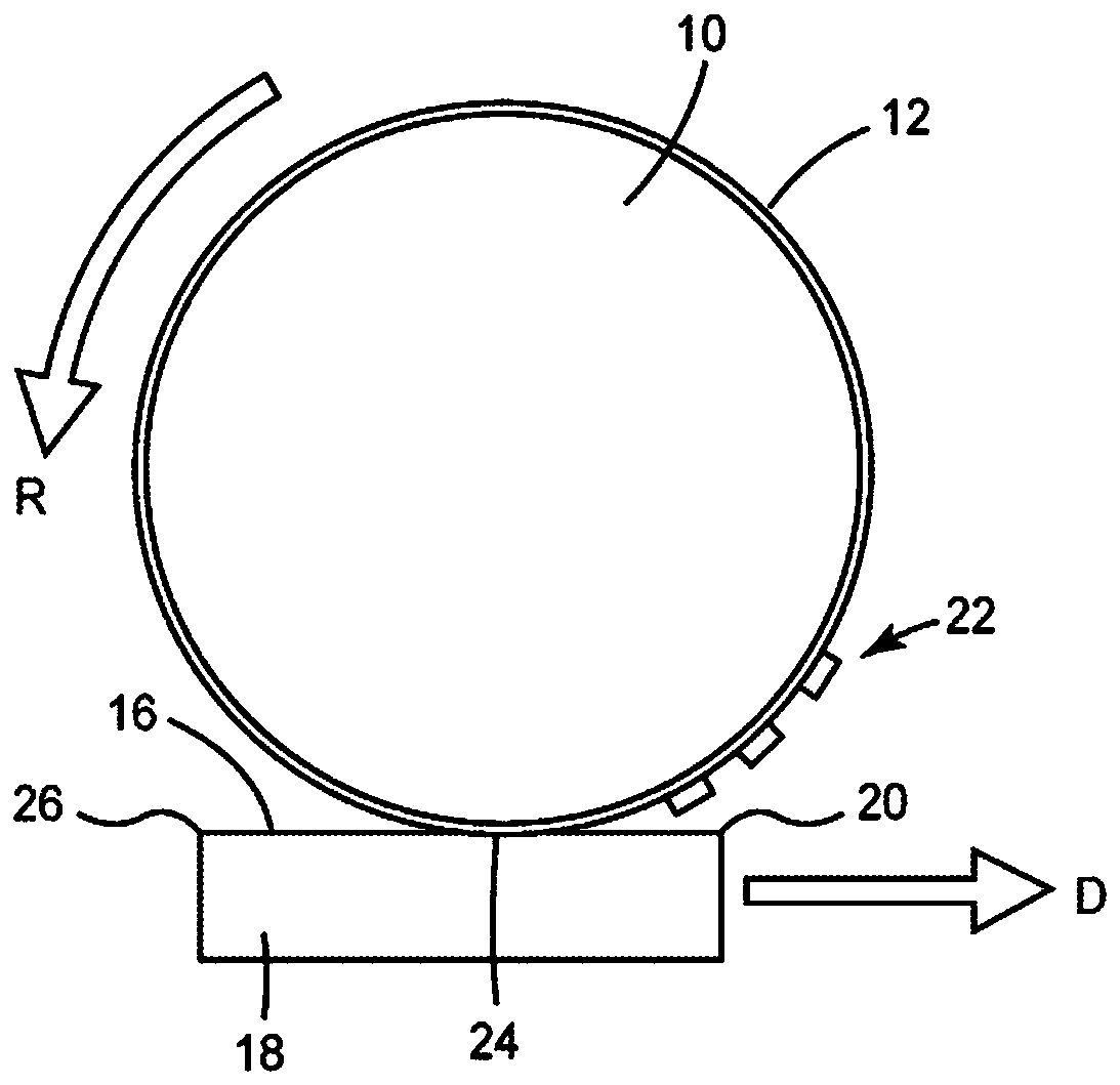
[0090] Attach the impression to the Figure 2A to Figure 2B The vacuum chucks in the imprint module are schematically shown in . Using an optical alignment method, align the tool to the tool coordinate system. Coordinates the surface velocity of the planar impression and tool substrate while actively maintaining alignment.
[0091] After initiation of contact between the stamp and tool substrate, a substantially constant contact force is maintained at the interface between the stamp surface and the non-planar surface, and when the stamp surface and the non-planar surface are in contact with each other, the interface is allowed to The contact pressure is varied until the entire stamp has been...
Embodiment 2
[0095] A tool layer of 1 μm diamond-like carbon (DLC) was coated onto the silicon wafer, followed by a 50 nm printed layer of gold.
[0096] Nanoscale patterns were hand-imprinted onto the printed layer, followed by chemical etching with a ferric nitrate / thiourea solution.
[0097] Then, include O 2 and C 6 f 14 Reactive ion etching (RIE) equipment of etching gas processes the printed wafer, where the gold printed layer is used as a mask.
[0098] Figure 8 The final structure in the DLC tools layer is shown in .
Embodiment approach A
[0100] Embodiment A. A method of applying a pattern to a non-planar surface, wherein at least a portion of the non-planar surface has a radius of curvature, the method comprising:
[0101] A stamp is provided having a major surface comprising a relief pattern of pattern elements extending away from a base surface, wherein each pattern element comprises an embossed surface with a lateral dimension greater than 0 and less than about 5 microns, and wherein the embossed a surface comprising ink having functionalized molecules having functional groups chemically bonded to said non-planar surface;
[0102] positioning the stamp to induce rolling contact between the non-planar surface and the major surface of the stamp;
[0103] contacting the embossed surface of the pattern element with the non-planar surface to form a self-assembled monolayer (SAM) of the functionalized molecules on the non-planar surface and impart to the non-planar surface arrangement of pattern elements; and
...
PUM
| Property | Measurement | Unit |
|---|---|---|
| Horizontal size | aaaaa | aaaaa |
| Horizontal size | aaaaa | aaaaa |
| Horizontal size | aaaaa | aaaaa |
Abstract
Description
Claims
Application Information
 - R&D
- Intellectual Property
- Life Sciences
- Materials
- Tech Scout
- Unparalleled Data Quality
- Higher Quality Content
- 60% Fewer Hallucinations
Browse by: Latest US Patents, China's latest patents, Technical Efficacy Thesaurus, Application Domain, Technology Topic, Popular Technical Reports.
© 2025 PatSnap. All rights reserved.Legal|Privacy policy|Modern Slavery Act Transparency Statement|Sitemap|About US| Contact US: help@patsnap.com