SHJ solar cell TCO film surface treatment method

A surface treatment and solar cell technology, applied in the field of solar cells, can solve problems such as sewage discharge and mask cost, silver-clad copper low-temperature paste printability, and product cost that do not meet the requirements of industrialization promotion, etc., to achieve easy control of the process, The effect of improving stability and product yield and reducing production cost

Active Publication Date: 2020-09-25
ZHONGWEI NEW ENERGY CHENGDU CO LTD
View PDF3 Cites 3 Cited by
  • Summary
  • Abstract
  • Description
  • Claims
  • Application Information

AI Technical Summary

Problems solved by technology

However, compared with the mature and low-cost screen printing technology, the copper electroplating technology faces the problems of sewage discharge and mask cost, the smart grid connection technology faces the problems of exclusive suppliers and patented technology, the printability of silver-coated copper low-temperature paste and the Product cost is not enough to promote industrialization

Method used


Image

  • SHJ solar cell TCO film surface treatment method
  • SHJ solar cell TCO film surface treatment method
  • SHJ solar cell TCO film surface treatment method

Examples


Embodiment 1

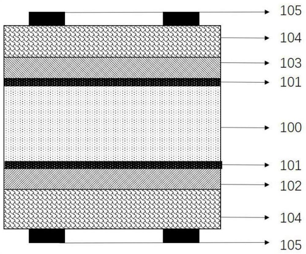
[0032] This embodiment takes the PECVE coating technology as an example to provide a surface treatment method for TCO thin films of SHJ solar cells, including the following steps:

[0033] (1) Using an n-type single crystal silicon wafer 100 as a substrate, first carry out surface texturing and chemical cleaning on the silicon wafer to form a pyramidal concave-convex structure that can improve light absorption on the surface, and then form an ultra-clean surface after chemical cleaning again, Then utilize the PECVD method to deposit intrinsic amorphous silicon film 101 on the upper and lower surfaces of the silicon wafer respectively, deposit a P-type doped silicon thin film 102 stack on the lower surface intrinsic amorphous silicon thin film 101, and deposit the intrinsic amorphous silicon thin film 101 on the upper surface Deposit an N-type doped amorphous silicon thin film 103 stack on the top, and then deposit a TCO thin film 104 on both sides respectively.
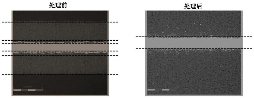
[0034](2) Aft...

Embodiment 2

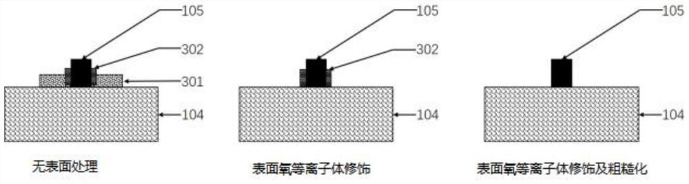
[0037] The difference between this embodiment and embodiment 1 is that, with O 2 As the plasma gas source, the surface of the TCO film was modified, but the roughening treatment was omitted, and the rest of the steps were the same.

Embodiment 3

[0039] The difference between this embodiment and embodiment 1 is that, with CCl 4 and Ar as the plasma gas source to roughen the surface of the TCO film. 2 and SF 6 Perform modification treatment for the plasma gas source, and the rest of the steps are the same.


PUM

PropertyMeasurementUnit
Surface roughnessaaaaaaaaaa
Surface energyaaaaaaaaaa
Thicknessaaaaaaaaaa

Abstract

The invention discloses an SHJ solar cell TCO film surface treatment method, which is used for solving the problem of poor contact between a TCO film and low-temperature silver paste in the prior art,and relates to the technical field of solar cells, and comprises the following steps: (1) depositing intrinsic amorphous silicon or amorphous silica films on the upper surface and the lower surface of a silicon wafer; (2) respectively depositing a P-type doped amorphous silicon film and an N-type doped amorphous silicon film on the upper surface and the lower surface of the silicon wafer obtainedin the step (1), or depositing amorphous silica films on the upper surface and the lower surface of the silicon wafer; (3) depositing TCO films on the upper surface and the lower surface of the silicon wafer obtained in the step (2); (4) carrying out surface treatment on the TCO film by adopting plasma, wherein the surface treatment comprises roughening treatment and modification treatment. According to the method, the contact between the low-temperature silver paste and the surface of the TCO thin film is better, the extension amount of the edge of the paste is low, the extension amount of organic matters in a paste system is small, the conversion efficiency of the SHJ solar cell is effectively improved, and the stability and the product yield of large-scale production of the SHJ solar cell are improved.

Description

technical field [0001] The invention discloses a surface treatment method for a TCO thin film of an SHJ solar cell, which belongs to the technical field of solar cells, and in particular relates to the surface treatment technology of a TCO thin film. Background technique [0002] Solar cell power generation (photovoltaic power generation) is one of the fastest-growing renewable energy technologies. As of the end of 2018, the global cumulative installed capacity has exceeded 400GW, becoming the main force of new energy. As the world's largest producer and installed capacity of solar cells, China's average growth rate has exceeded 140% in the past 10 years, and its cumulative installed capacity is close to 200GW, making it a veritable photovoltaic powerhouse. In recent years, with the rapid expansion and development of the entire photovoltaic industry chain, industrialization technology innovation and the support of relevant national preferential policies, compared with 10 yea...

Claims


Application Information

Patent Timeline
IPC IPC(8): H01L31/20H01L31/0216H01L31/0236H01L31/074
CPCH01L31/202H01L31/208H01L31/02168H01L31/02366H01L31/074Y02E10/50Y02P70/50
Inventor 石建华孟凡英韩安军张丽平刘正新谢毅
Owner ZHONGWEI NEW ENERGY CHENGDU CO LTD
Why Eureka
Try Eureka