
Method for increasing roughness on semiconductor surface

A semiconductor and roughness technology, which is applied in the manufacture of semiconductor/solid-state devices, electrical components, circuits, etc., can solve the problems of low etching selectivity, damage to semiconductor components, and roughness that is difficult to achieve roughness, so as to avoid the formation of excessive etching , slow down the etching speed, increase the effect of roughness

Pending Publication Date: 2020-09-29
SAE TECH DELEVOPMENT DONGGUAN
View PDF0 Cites 0 Cited by
  • Summary
  • Abstract
  • Description
  • Claims
  • Application Information

AI Technical Summary

Problems solved by technology

Although this traditional etching method can form a rough surface on the semiconductor surface, yet, because this ion etching is mainly a physical process, and in the physical etching process, the above-mentioned ionized processing gases (argon, oxygen) have a negative effect on aluminum oxide and carbonization. The difference in the etching rate of titanium is not large, that is, the etching selectivity (alumina / titanium carbide) is small, so that other components of the semiconductor are damaged
Moreover, the roughness formed is difficult to achieve the required roughness

Method used


Image

  • Method for increasing roughness on semiconductor surface
  • Method for increasing roughness on semiconductor surface

Examples


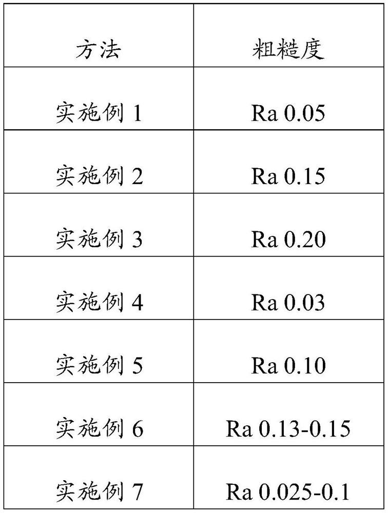
Embodiment 1

[0021] As a method for increasing roughness on a semiconductor surface according to an embodiment of the present invention, the method includes the following steps:

[0022] (1) Provide a semiconductor and determine the area where the roughness of the semiconductor surface is to be increased, denoted as area A, and the thickness of the photoresist is 10 μm;

[0023] (2) use photoresist to shield the semiconductor surface except other parts of area A;

[0024] (3) Load the semiconductor processed in step (2) into the semiconductor processing chamber, and form a vacuum in the processing chamber with a vacuum degree of 0.000006 Toor, and introduce a mixture of inert gas and hydrocarbon gas into the processing chamber to maintain the processing The chamber vacuum is 0.004 Toor, and the mixed gas is ionized to form an ion beam for etching; the inert gas is argon, the hydrocarbon gas is ethylene, and the volume ratio of argon in the mixed gas is 85%. The etching time is 30-45 minut...

Embodiment 2

[0027] As a method for increasing roughness on the surface of a semiconductor according to an embodiment of the present invention, the only difference between this embodiment and Embodiment 1 is that the volume ratio of argon in the mixed gas is 90%.

Embodiment 3

[0029] As a method for increasing roughness on a semiconductor surface in an embodiment of the present invention, the only difference between this embodiment and Embodiment 1 is that the volume ratio of argon in the mixed gas is 95%.


PUM

PropertyMeasurementUnit
Thicknessaaaaaaaaaa

Abstract

The invention provides a method for increasing roughness on a semiconductor surface. The method comprises the following steps: providing a semiconductor and shielding a part, except for a to-be-increased roughness region, of the semiconductor surface by using photoresist; and loading the processed semiconductor into a semiconductor processing chamber, forming a vacuum in the processing chamber, introducing a mixed gas of an inert gas and a hydrocarbon gas into the processing chamber, and ionizing the mixed gas to form an ion beam for etching, wherein the inert gas is argon, the hydrocarbon gasis ethylene, and the volume ratio of argon in the mixed gas is 85%-95%. According to the method, the area outside the area, where roughness needs to be increased, of the surface of the semiconductoris shielded through the photoresist, ion beams are formed under the vacuum condition for etching to increase the roughness of the surface of the semiconductor, and the method is simple and low in cost; and in the mixed gas forming the ion beam, ethylene plays a role in dilution, thereby facilitating reducing the etching speed so as to avoid forming excessive etching.

Description

technical field [0001] The invention relates to the field of semiconductor processing, in particular to a method for increasing roughness on a semiconductor surface. Background technique [0002] In microelectronics, some operations require the bonding surface to be as smooth as possible, but some components need to manufacture surfaces that face each other but do not adhere to each other, so as to prevent the semiconductor from being unsmooth on the corresponding object surface. Properly bonded and able to maintain its gliding properties. [0003] Conventional methods of roughening surfaces are usually carried out by means of such ion bombardment, also known as ion beam milling. During the etching process, there is almost no chemical reaction between the ion beam and the semiconductor surface material, but a kind of momentum transfer (momentum transfer). Although this traditional etching method can form a rough surface on the semiconductor surface, yet, because this ion e...

Claims


Application Information

Patent Timeline
IPC IPC(8): H01L21/3065
CPCH01L21/3065
Inventor 肖荣健
Owner SAE TECH DELEVOPMENT DONGGUAN
Learn More