Detection medium and preparation method thereof and diamond detector

A diamond and detector technology, which is applied in the field of semiconductor detectors, can solve the problems of increased dark current of detectors, difficulty in achieving high-dose doping, and hindering diamond sensitivity.

Active Publication Date: 2020-09-29
NINGBO INST OF MATERIALS TECH & ENG CHINESE ACADEMY OF SCI
View PDF8 Cites 2 Cited by
  • Summary
  • Abstract
  • Description
  • Claims
  • Application Information

AI Technical Summary

Problems solved by technology

However, the multi-layer electrode structure built on the reaction surface of diamond will greatly hinder the sensitivity of diamond to external responsive signals, so that the effective area of ​​the reaction surface that can respond to detection signals is greatly reduced, the dark current of the detector increases, and the sensitivity of the device is greatly reduced. very unfavorable
Moreover, it is difficult to achieve high-dose doping on the surface of diamond, so it is quite difficult to make electrodes with good ohmic contact on diamond

Method used


Image

  • Detection medium and preparation method thereof and diamond detector
  • Detection medium and preparation method thereof and diamond detector
  • Detection medium and preparation method thereof and diamond detector

Examples


preparation example Construction

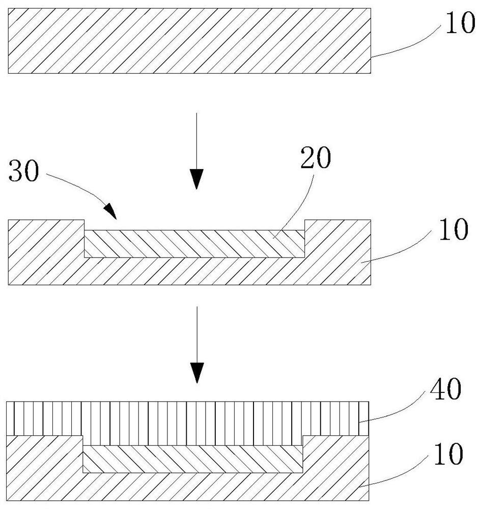
[0031] Such as figure 1 Shown, the preparation method of detection medium provided by the present invention comprises the following steps:

[0032] S1, providing a single crystal diamond substrate 10;

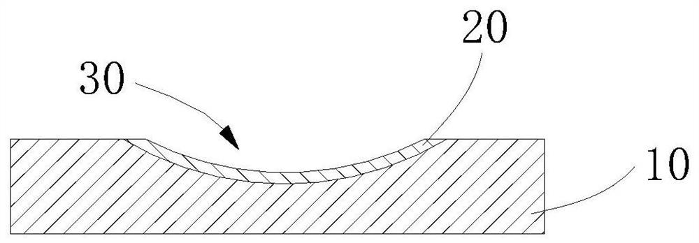
[0033] S2, using a laser to directly write the surface of the diamond substrate 10, so that the diamond is transformed into a graphite layer 20 in situ, wherein the surface of the graphite layer 20 is lower than the surface of the diamond substrate 10 and formed from the diamond substrate 10 The surface extends to the groove 30 of the graphite layer 20, the groove 30 has a width of 1 μm to 60 μm, a depth of 20 μm to 100 μm, and a length not less than 1 / 4 of the shortest dimension of the surface of the diamond substrate 10;

[0034] S3, epitaxially growing a single crystal diamond layer 40 on the diamond substrate 10, and making the single crystal diamond layer 40 cover at least the graphite layer 20 to obtain a detection medium.

[0035] In step S1, the shape of the surface o...

Embodiment 1

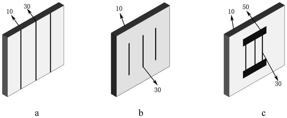
[0064] A groove is directly written on the upper surface of the HPHT single crystal diamond substrate with a size of 3.5mm×3.5mm×1mm. The laser beam spot diameter is 10μm, the power is 350W, and the scanning speed is 1000mm / s. The width is about 50 μm, the depth is about 20 μm, and the length is about 1.5 mm. The grooved diamond substrate was subjected to surface morphology analysis and Raman spectrum analysis, the results are as follows Figure 4 with Figure 5 shown. Depend on Figure 5 It can be seen that there is a graphite layer in the groove after laser direct writing, and the graphite layer is formed by in-situ transformation of diamond. The electrical conductivity test shows that the resistance of the graphite layer is about 25Ω / cm.

[0065] Then, the diamond substrate with grooves was ultrasonicated in an ethanol solution for 10 minutes, and then placed in the growth chamber of the MPCVD equipment, vacuumed to a pressure of 0.1 Pa in the growth chamber, and preheat...

Embodiment 2

[0068] Two grooves are directly written on the upper surface of the HPHT single crystal diamond substrate with a size of 3.5mm×3.5mm×1mm. The laser beam spot diameter is 5μm, the power is 350W, and the scanning speed is 1000mm / s. The width is about 50 μm, the depth is about 40 μm, the length is about 1.5 mm, and the pitch is 1 mm. After laser direct writing, there is a graphite layer in the groove, which is formed by in-situ transformation of diamond. The electrical conductivity test shows that the resistance of the graphite layer is about 28Ω / cm.

[0069] Then, the diamond substrate with grooves was ultrasonicated in an ethanol solution for 10 minutes, and then placed in the growth chamber of the MPCVD equipment, vacuumed to a pressure of 0.1 Pa in the growth chamber, and preheated for 1 minute. Then, hydrogen gas was introduced at a flow rate of 410 sccm. Simultaneously, increase the pressure of the growth chamber and the power of the microwave synchronously until the press...


PUM

PropertyMeasurementUnit
depthaaaaaaaaaa
thicknessaaaaaaaaaa

Abstract

The invention relates to a detection medium and a preparation method thereof and a diamond detector. The preparation method comprises the following steps: providing a monocrystalline diamond matrix; carrying out laser direct writing on the surface of the diamond matrix, so that the diamond is converted into a graphite layer in situ, wherein the surface of the graphite layer is lower than the surface of the diamond matrix to form a groove extending from the surface of the diamond matrix to the graphite layer, the width of the groove ranging from 1 micrometer to 60 micrometers, the depth of thegroove ranging from 20 micrometers to 100 micrometers, and the length of the groove being not smaller than 1 / 4 of the shortest size of the surface of the diamond matrix; and epitaxially growing a single crystal diamond layer on the diamond matrix, and enabling the single crystal diamond layer to at least cover the graphite layer to obtain the detection medium. In the detection medium obtained by the invention, the monocrystalline diamond layer plays a detection role, so that the effective area of the diamond for detection response is increased; and when the detection medium is applied to the diamond detector, the sensitivity of the diamond detector to external responsive signals can be improved.

Description

technical field [0001] The invention relates to the field of semiconductor detectors, in particular to a detection medium, a preparation method thereof, and a diamond detector. Background technique [0002] Semiconductor detectors are radiation detectors with semiconductor materials as the detection medium, and for semiconductor detectors made of diamond, whether it is to transport the electron-hole carriers generated by the action of external signals on diamond to Whether the external circuit forms the collection of electrical signals, or realizes the recombination of internal electron-hole carrier pairs by applying an electric field to it, it is necessary to add suitable electrodes to the diamond to form a good electrical contact between the electrodes and the diamond- Non-rectifying (ohmic) contacts. [0003] However, due to the large forbidden band width of diamond, it is easy to form a Schottky rectifying contact due to the interface barrier when it is in contact with ...

Claims


Application Information

Patent Timeline
Patent Type & Authority Applications(China)
IPC IPC(8): H01L31/028H01L31/09H01L31/18H01L21/02
CPCH01L31/028H01L31/09H01L31/1804H01L21/02376H01L21/02527H01L21/0262H01L21/02664Y02P70/50
Inventor 江南林正得杨明阳高靖尧戴丹
Owner NINGBO INST OF MATERIALS TECH & ENG CHINESE ACADEMY OF SCI
Why Eureka
Try Eureka