SiGe HBT (Heterojunction Bipolar Transistor) device strain Si BiCMOS (Bipolar Complementary Metal Oxide Semiconductor) integrated device and manufacturing method thereof

A technology for integrating devices and devices, which is used in semiconductor/solid-state device manufacturing, electric solid-state devices, semiconductor devices, etc., and can solve problems such as low mechanical strength, complex preparation process, and incompatibility with wide-ranging applications and development.

Inactive Publication Date: 2015-07-22
XIDIAN UNIV
View PDF1 Cites 0 Cited by
  • Summary
  • Abstract
  • Description
  • Claims
  • Application Information

AI Technical Summary

Problems solved by technology

Although GaAs and InP-based compound devices have superior frequency characteristics, their preparation process is more complicated than Si process, high cost, difficult to prepare large-diameter single crystal, low mechanical strength, poor heat dissipation performance, incompatibility with Si process and lack of SiO 2 Such passivation layer and other factors limit its wide application and development.

Method used


Image

  • SiGe HBT (Heterojunction Bipolar Transistor) device strain Si BiCMOS (Bipolar Complementary Metal Oxide Semiconductor) integrated device and manufacturing method thereof

Examples


Embodiment 1

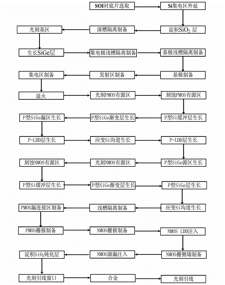
[0128] Embodiment 1: SiGe HBT devices, strained Si BiCMOS integrated devices and circuits with a channel length of 22nm are prepared, and the specific steps are as follows:

[0129] Step 1, epitaxial material preparation.

[0130] (1a) Select the doping concentration as 5×10 14 cm -3 A P-type Si sheet as a substrate;

[0131] (1b) Using chemical vapor deposition (CVD), at 600°C, deposit a SiO with a thickness of 300nm on the surface of the epitaxial Si layer. 2 Layer, photolithographic buried layer region, N-type impurities are implanted into the buried layer region to form N-type heavily doped buried layer region;

[0132] (1c) Etch the oxide layer on the surface of the substrate, and use chemical vapor deposition (CVD) to grow an N-type epitaxial Si layer with a thickness of 1.5 μm on the upper Si material at 600 ° C, as a set electrical region, the doping concentration of this layer is 1×10 16 cm -3 ;

[0133] (1d) Deposit a layer of SiO with a thickness of 200nm on ...

Embodiment 2

[0204] Embodiment 2: The SiGe HBT device, the strained Si BiCMOS integrated device and the circuit that the channel length is prepared to be 30nm, the specific steps are as follows:

[0205] Step 1, epitaxial material preparation.

[0206] (1a) Select the doping concentration as 1×10 15 cm -3 A P-type Si sheet as a substrate;

[0207](1b) Using chemical vapor deposition (CVD), at 700 ° C, deposit a SiO with a thickness of 400 nm on the surface of the epitaxial Si layer. 2 Layer, photolithographic buried layer region, N-type impurities are implanted into the buried layer region to form N-type heavily doped buried layer region;

[0208] (1c) Etch the oxide layer on the surface of the substrate, and use chemical vapor deposition (CVD) to grow a layer of N-type epitaxial Si layer with a thickness of 1.8 μm on the upper Si material at 700 ° C, as a set electrical region, the doping concentration of this layer is 5×10 16 cm -3 ;

[0209] (1d) Deposit a layer of SiO with a thi...

Embodiment 3

[0280] Embodiment 3: The SiGe HBT device, the strained Si BiCMOS integrated device and the circuit that the channel length is prepared to be 45nm, the specific steps are as follows:

[0281] Step 1, epitaxial material preparation.

[0282] (1a) Select the doping concentration as 5×10 15 cm -3 A P-type Si sheet as a substrate;

[0283] (1b) Using chemical vapor deposition (CVD), at 800 ° C, deposit a SiO with a thickness of 500 nm on the surface of the epitaxial Si layer. 2 Layer, photolithographic buried layer region, N-type impurities are implanted into the buried layer region to form N-type heavily doped buried layer region;

[0284] (1c) Etch the oxide layer on the surface of the substrate, and use chemical vapor deposition (CVD) to grow a layer of N-type epitaxial Si layer with a thickness of 2.5 μm on the upper Si material at 750 ° C, as a set electrical region, the doping concentration of this layer is 1×10 17 cm -3 ;

[0285] (1d) Deposit a layer of SiO with a th...


PUM

PropertyMeasurementUnit
thicknessaaaaaaaaaa
thicknessaaaaaaaaaa
thicknessaaaaaaaaaa

Abstract

The invention discloses a SiGe HBT (Heterojunction Bipolar Transistor) device strain Si BiCMOS (Bipolar Complementary Metal Oxide Semiconductor) integrated device and a manufacturing method of the SiGe HBT device strain Si BiCMOS integrated device. The method comprises the following steps of: growing N-Si on an Si substrate as a bipolar device collector region; etching a base region; growing P-SiGe, i-Si, i-Poly-Si in the base region; manufacturing deep trench isolation; manufacturing an emitter, a base and a collector; forming a SiGe HBT device; etching an active area trench of an NMOS (N-Channel Metal Oxide Semiconductor) device and a PMOS (P-Channel Metal Oxide Semiconductor) device respectively; growing an active layer at the NMOS and PMOS devices at the active area trench of the NMOS and PMOS devices respectively; manufacturing the source and drain and the grid of the NMOS and PMOS devices respectively so as to form the NMOS and PMOS devices; and alloying and etching a lead so as to form the SiGe HBT device, the strain Si BiCMOS integrated device and a circuit. The characteristic of anisotropic tension strain Si material mobility rate is utilized sufficiently; and the SiGe HBT device, and the strain Si BiCMOS integrated circuit with enhanced performance are manufactured at 600-800 DEG C.

Description

technical field [0001] The invention belongs to the technical field of semiconductor integrated circuits, and in particular relates to a strained SiBiCMOS integrated device of a SiGe HBT device and a preparation method thereof. Background technique [0002] Integrated circuits are the cornerstone and core of the economic development of an information society. Just as the American engineering and technology circle recently named the fifth electronic technology among the 20 greatest engineering and technological achievements in the world in the 20th century, "from vacuum tubes to semiconductors and integrated circuits, they have become the cornerstone of intelligent work in various industries today." Integrated circuits. It is one of the typical products that can best reflect the characteristics of knowledge economy. At present, the electronic information industry based on integrated circuits has become the world's largest industry. With the development of integrated circuit...

Claims


Application Information

Patent Timeline
Patent Type & Authority Patents(China)
IPC IPC(8): H01L27/06H01L21/8249
Inventor 胡辉勇宋建军张鹤鸣舒斌李妤晨吕懿宣荣喜郝跃
Owner XIDIAN UNIV
Why Eureka
Try Eureka