ITO thin film
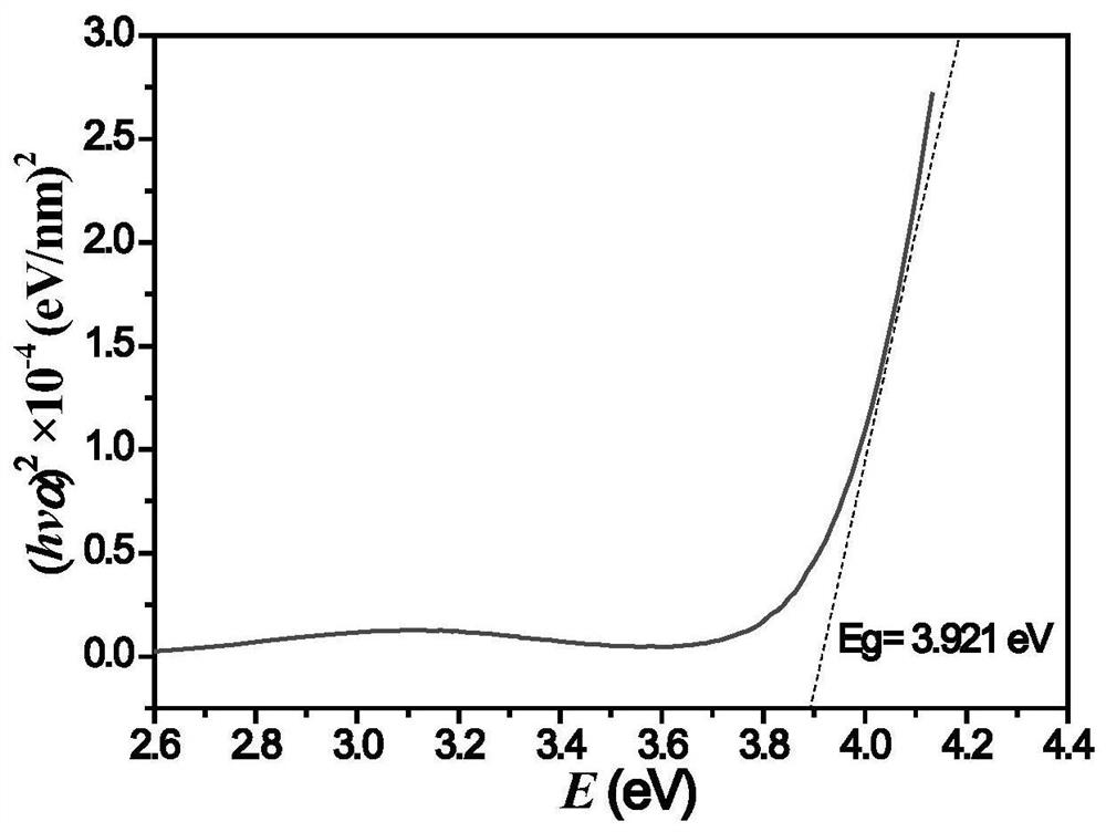
A technology of thin film and variable temperature buffering, which is applied in the direction of ion implantation plating, metal material coating process, coating, etc., can solve the problem of affecting the electron mobility and optical properties of thin films, the reduction of electron mean free path and optical bandgap, nanometer Difficult to control the order of magnitude film thickness, etc., to achieve the effect of high carrier concentration and mobility, wide band gap, and wide Eg
- Summary
- Abstract
- Description
- Claims
- Application Information
AI Technical Summary
Problems solved by technology
Method used
Image
Examples
Embodiment 1
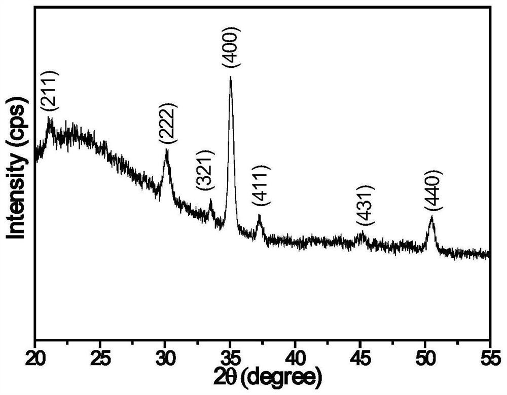
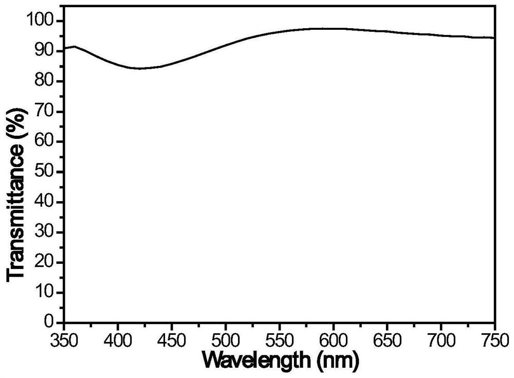
[0027] A kind of ITO thin film, comprises temperature-variable buffer layer and orientation growth layer, and wherein temperature-variable buffer layer is ITO polycrystalline thin film homogeneous buffer layer, adopts magnetron sputtering growth, through the temperature gradient in the sputtering growth process, makes buffer layer have ( 004) preferred orientation, the thickness of the temperature-variable buffer layer is 20 nm, and the carrier concentration of the temperature-variable buffer layer is 1E18 cm at 300 K -3 , electron mobility at 50 cm 2 / Vs, the average transmittance of visible light at 300 K is 95%. The oriented growth layer is grown by magnetron sputtering, and continues to inherit the (004) orientation of the temperature-changing buffer layer. The thickness of the oriented growth layer is 20 nm, and the carrier concentration of the oriented growth layer is 1E18cm at 300 K. -3 , electron mobility 50 cm 2 / Vs, the visible light transmittance of the oriented g...
Embodiment 2
[0030] A kind of ITO thin film, comprises temperature-variable buffer layer and orientation growth layer, and wherein temperature-variable buffer layer is ITO polycrystalline thin film homogeneous buffer layer, adopts magnetron sputtering growth, through the temperature gradient in the sputtering growth process, makes buffer layer have ( 004) preferred orientation, the thickness of the temperature-variable buffer layer is 50 nm, and the carrier concentration of the temperature-variable buffer layer is 1E21 cm at 300 K -3 , electron mobility is 30 cm 2 / Vs, the average transmittance of visible light at 300 K is 90%. The oriented growth layer is grown by magnetron sputtering, and continues to inherit the (004) orientation of the temperature-variable buffer layer. The thickness of the oriented growth layer is 200 nm, and the carrier concentration of the oriented growth layer is 1E21cm at 300 K. -3 , electron mobility 30 cm 2 / Vs. The visible light transmittance of the oriented...
Embodiment 3
[0033] A kind of ITO thin film, comprises temperature-variable buffer layer and orientation growth layer, and wherein temperature-variable buffer layer is ITO polycrystalline thin film homogeneous buffer layer, adopts magnetron sputtering growth, through the temperature gradient in the sputtering growth process, makes buffer layer have ( 004) preferred orientation, the thickness of the temperature-variable buffer layer is 100 nm, and the carrier concentration of the temperature-variable buffer layer is 1E22 cm at 300 K -3 , the electron mobility is 20 cm 2 / Vs, the average visible light transmittance of the buffer layer at 300 K is 85%. The oriented growth layer is grown by magnetron sputtering, and continues to inherit the (004) orientation of the variable temperature buffer layer. The thickness of the oriented growth layer is 1000 nm, and the carrier concentration of the oriented growth layer is 1E22 cm at 300 K. -3 , electron mobility 20 cm 2 / Vs. The average visible lig...
PUM
| Property | Measurement | Unit |
|---|---|---|
| thickness | aaaaa | aaaaa |
| thickness | aaaaa | aaaaa |
| thickness | aaaaa | aaaaa |
Abstract
Description
Claims
Application Information


