A method of making doped amorphous silicon on the back of hbc battery

A technology of amorphous silicon and hydrogenated amorphous silicon, which is applied in the manufacture of circuits, electrical components, and final products, can solve the problems of complex process flow, high production cost, and many process steps, and increase the window and machine cost. Reduction, the effect of reducing operating costs

Active Publication Date: 2022-03-29
普乐新能源科技(泰兴)有限公司
View PDF6 Cites 0 Cited by
  • Summary
  • Abstract
  • Description
  • Claims
  • Application Information

AI Technical Summary

Problems solved by technology

At present, HBC solar cells have not yet achieved large-scale industrialization, and its complex process and high production costs are the main reasons for the lack of large-scale production.
The complex process is mainly to make the N-type a-Si:H layer and the P-type a-Si:H layer in the finger-like cross distribution on the back, and the process steps are many and complicated.

Method used


Image

  • A method of making doped amorphous silicon on the back of hbc battery
  • A method of making doped amorphous silicon on the back of hbc battery
  • A method of making doped amorphous silicon on the back of hbc battery

Examples


Embodiment 1

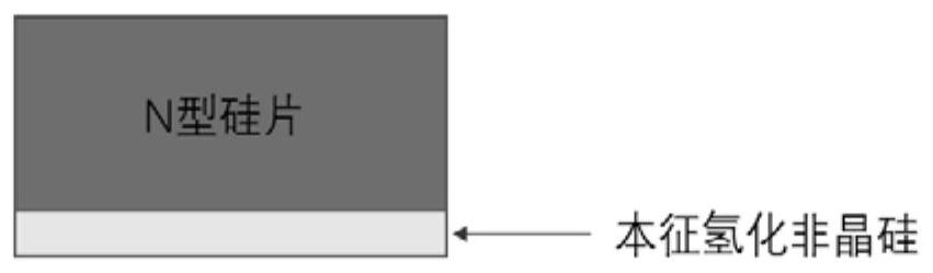
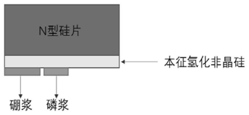
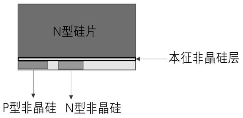
[0036] Such as Figure 1-6 Shown, a kind of method for making HBC cell back doped amorphous silicon, comprises the following steps:

[0037] (1) The intrinsic hydrogenated amorphous silicon layer (i-a-Si: H) is grown by PECVD on the back of the N-type polished wafer, the deposition temperature is 200°C, the deposition power is 50W, the deposition pressure is 200Pa, and hydrogen and silane are introduced. The growth thickness is about 100nm, of which 10nm is used as a passivation layer on the back surface, and the rest is used as a doped amorphous silicon layer.

[0038] (2) Print boron paste on the amorphous silicon layer, the printed pattern is consistent with the screen pattern in the P area of ​​the metallized electrode, and dry at 100° C. for 5 minutes. In some preferred manners, the printing width can be adjusted according to the line width of the screen.

[0039] (3) Phosphorus paste is printed on the amorphous silicon layer, and the printed pattern is consistent with ...

Embodiment 2

[0046] Such as Figure 1-6Shown, a kind of method for making HBC cell back doped amorphous silicon, comprises the following steps:

[0047] (1) An intrinsic hydrogenated amorphous silicon layer (i-a-Si: H) is grown on the back of the N-type polished wafer, with a thickness of about 120nm, of which 10nm is used as a passivation layer on the back surface, and the rest is used as doped amorphous silicon Floor.

[0048] (2) Print boron paste on the amorphous silicon layer, the printed pattern is consistent with the screen pattern in the P area of ​​the metallized electrode, and dry at 100° C. for 5 minutes.

[0049] (3) Phosphorus paste is printed on the amorphous silicon layer, and the printed pattern is consistent with the screen pattern in the N area of ​​the metallized electrode, and dried at 100° C. for 5 minutes.

[0050] (4) Put the printed silicon chip into the laser for laser doping, and obtain the required square resistance of the P area and the N area, wherein, the P ...

Embodiment 3

[0055] Such as Figure 1-6 Shown, a kind of method for making HBC cell back doped amorphous silicon, comprises the following steps:

[0056] (1) An intrinsic hydrogenated amorphous silicon layer (i-a-Si: H) is grown on the back of the N-type polished wafer, with a thickness of about 150nm, of which 15nm is used as a passivation layer on the back surface, and the rest is used as doped amorphous silicon Floor.

[0057] (2) Print boron paste on the amorphous silicon layer, the printed pattern is consistent with the screen pattern in the P area of ​​the metallized electrode, and dry at 100° C. for 5 minutes.

[0058] (3) Phosphorus paste is printed on the amorphous silicon layer, and the printed pattern is consistent with the screen pattern in the N area of ​​the metallized electrode, and dried at 100° C. for 5 minutes.

[0059] (4) Put the printed silicon chip into the laser for laser doping, and obtain the required square resistance of the P area and the N area, wherein, the P...


PUM

PropertyMeasurementUnit
thicknessaaaaaaaaaa
thicknessaaaaaaaaaa
thicknessaaaaaaaaaa

Abstract

The invention provides a method for making the back of an HBC cell doped with amorphous silicon, comprising: growing an intrinsic hydrogenated amorphous silicon layer on the back of an N-type polished silicon wafer; printing boron paste on the hydrogenated amorphous silicon layer, Drying; printing phosphorous paste on the hydrogenated amorphous silicon layer, drying; putting the printed silicon wafer into the laser for laser doping, to obtain the required square resistance of the P area and the N area; giving the surface of the cell A mask is plated as a polishing barrier; the position between the P region and the N region is cut with a laser, and the mask in the middle is removed. The method of the invention can ensure the uniformity and growth rate of the back doped amorphous silicon.

Description

technical field [0001] The invention relates to a solar energy HBC cell manufacturing process, in particular to a method for manufacturing the back side of the HBC cell doped with amorphous silicon. Background technique [0002] As the three pillars of social development, energy is not only the driving force for the development and development of human production activities, but also plays a huge role in promoting the development of human society and economy. For decades, countries around the world have vigorously exploited fossil fuels for their own development. However, the excessive use of fossil fuels has caused serious air pollution, which has become a major global problem. In order to cope with the impact of traditional fossil energy on the environment, it is necessary to reduce the proportion of traditional fossil energy consumption and develop green energy such as solar energy, wind energy and biomass. Among them, solar energy, as an ideal renewable energy source, ...

Claims


Application Information

Patent Timeline
Patent Type & Authority Patents(China)
IPC IPC(8): H01L31/18H01L31/0216H01L21/225H01L21/268
CPCH01L31/1804H01L31/02167H01L21/225H01L21/268Y02P70/50
Inventor 欧文凯
Owner 普乐新能源科技(泰兴)有限公司
Why Eureka
Try Eureka