Ink composition, packaging structure and semiconductor device

A composition and ink technology, applied in semiconductor devices, semiconductor/solid-state device manufacturing, semiconductor/solid-state device parts, etc., can solve the problems of low curing shrinkage rate and inability to take into account high light curing rate and other problems

Pending Publication Date: 2020-10-27
HANGZHOU FIRST APPLIED MATERIAL CO LTD
View PDF3 Cites 6 Cited by
  • Summary
  • Abstract
  • Description
  • Claims
  • Application Information

AI Technical Summary

Problems solved by technology

[0012] The main purpose of the present invention is to provide an ink composition, packaging structure and semiconductor device to solve the problem that the film packaging materials in the prior art cannot take into account the high photocuring rate and low curing shrinkage

Method used


Image

  • Ink composition, packaging structure and semiconductor device
  • Ink composition, packaging structure and semiconductor device
  • Ink composition, packaging structure and semiconductor device

Examples


Embodiment 1

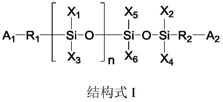
[0068] In a 1000 mL flask with a cooling tube and a stirrer, put 800 mL of toluene, 60 g of 1,1,5,5-tetramethyl-3,3-diphenyltrisiloxane, and 100 g of allyl alcohol, followed by nitrogen Purge for 60 minutes. After that, 0.0063 g of platinum(0)-1,3-diethylene-1,1,3,3-tetramethyldisiloxane was put into the flask, and the temperature of the flask was increased to 70° C., followed by stirring 5h. Residual solvent was removed by distillation. Further, 79 g of the obtained compound was introduced into a high-pressure reaction vessel, and after adding 400 mL of dichloromethane, 39.64 g of triethylamine was added thereto, followed by slowly introducing 90 g of vinyl chloride while stirring at 0°C. The residual solvent was removed by distillation, and 40 g of the product was obtained by column chromatography with a yield of 51%. Thus, a compound represented by Formula 1 was prepared, denoted as A1, and its purity was 98% as determined by HPLC. m / e:500.22; 1 HNMR (400MHz, Chloroform...

Embodiment 2

[0072] In a 1000mL flask with a cooling tube and a stirrer, put 800mL of toluene, 40g of 1,1,5,5-tetramethyl-3,3-diphenyltrisiloxane and 80g of allyl alcohol, followed by nitrogen blowing Sweep for 60 minutes. After that, 0.013 g of platinum(0)-1,3-diethylene-1,1,3,3-tetramethyldisiloxane was put into the flask, and the temperature of the flask was increased to 70° C., followed by stirring 5 hours. Residual solvent was removed by distillation. After introducing 71.2 g of the obtained compound into 300 mL of dichloromethane, 15 g of triethylamine was added thereto, followed by slowly introducing 40 g of methacryloyl chloride while stirring at 0°C. The residual solvent was removed by distillation, and the unilateral compound terminated by methacrylate group was obtained by column chromatography separation. The unilateral compound was introduced into a high-pressure reactor, 40 g of vinyl chloride was added, and 10 g of potassium carbonate was added. After reacting for 3 hours,...

Embodiment 3

[0076] In a 1000 mL flask with cooling tube and stirrer, put 800 mL of toluene, 54.11 g of 1,1,3,5,5-pentamethyl-3-phenyltrisiloxane and 100 g of allyl alcohol, followed by nitrogen Purge for 60 minutes. After that, 0.0063 g of platinum(0)-1,3-diethylene-1,1,3,3-tetramethyldisiloxane was put into the flask, and the temperature of the flask was increased to 70° C., followed by stirring 5h. Residual solvent was removed by distillation. Further, 79 g of the obtained compound was introduced into a high-pressure reaction vessel, and after adding 400 mL of dichloromethane, 39.64 g of triethylamine was added thereto, followed by slowly introducing 90 g of vinyl chloride while stirring at 0°C. Residual solvent was removed by distillation, and 40 g of the product was obtained by column chromatography with a yield of 51%, thus preparing a compound represented by formula 3, denoted as A3, with a purity of 97% as determined by HPLC, m / e: 588.24; 1 H NMR (400MHz, Chloroform-d)δ7.54(m,1H...


PUM

PropertyMeasurementUnit
viscosityaaaaaaaaaa

Abstract

The invention provides an ink composition, a packaging structure and a semiconductor device. The ink composition comprises a photocurable silicon-containing monomer component, an active diluent component and a photoinitiator component, wherein the photocurable silicon-containing monomer component is a photocurable silicon-containing monomer or a combination of a plurality of photocurable silicon-containing monomers, and each photocurable silicon-containing monomer has the following structural formula I: at least one of A1 and A2 in the photocurable silicon-containing monomer component is represented by any one of structural formulas II. According to the invention, when the silicon-containing monomer containing the alkenyl ether bond and the component containing the reactive diluent are matched for use, the free radical-cation hybrid curing system can be formed, and the free radical-cation hybrid curing system can reduce oxygen inhibition, improve the curing speed and reduce the curingshrinkage rate, so that the photocuring rate of the system can be improved, and the curing shrinkage rate of the system can be reduced; and thus, the organic barrier layer with relatively high photocuring rate and relatively low curing shrinkage rate is obtained.

Description

technical field [0001] The invention relates to the technical field of packaging materials, in particular to an ink composition, a packaging structure and a semiconductor device. Background technique [0002] Organic Light-Emitting Diodes (OLEDs) have the characteristics of all solid state, active light emission, high brightness, high contrast, ultra-thin and ultra-light, low cost, low power consumption, no viewing angle limitation, wide operating temperature range, etc. , and can be fabricated on a flexible, lightweight, and durable plastic substrate, which can realize a truly flexible display, and is a technology that best meets people's requirements for future displays. [0003] Various types of light-emitting diodes currently used mainly include organic small molecule light-emitting diodes (OLEDs), polymer organic light-emitting diodes (POLEDs), organic phosphorescent light-emitting diodes (PHOLEDs) and organic thermally stimulated delayed emission materials (TADF). How...

Claims


Application Information

Patent Timeline
Patent Type & Authority Applications(China)
IPC IPC(8): C09D11/30C09D11/101H01L23/29H01L31/0203H01L31/048H01L33/56H01L51/52
CPCC09D11/30C09D11/101H01L23/296H01L31/0203H01L31/0481H01L33/56H10K50/844Y02E10/50
Inventor 洪海兵
Owner HANGZHOU FIRST APPLIED MATERIAL CO LTD
Why Eureka
Try Eureka