Method for manufacturing high-integration microarray LED packaging module

A technology of LED packaging and manufacturing methods, applied in the direction of electrical components, electric solid devices, circuits, etc., can solve the problems of process complexity, high junction temperature, and affecting heat dissipation

Inactive Publication Date: 2020-10-27
石家庄费米原科技有限公司
View PDF0 Cites 1 Cited by
  • Summary
  • Abstract
  • Description
  • Claims
  • Application Information

AI Technical Summary

Problems solved by technology

[0003] There are four main problems in the existing technology: First, the existing LED epitaxial carrier substrate needs to do ion distribution on the semiconductor substrate wafer in order to conduct electricity, and also needs to make a positive electrode at the bottom of the LED epitaxial carrier substrate. The complexity and cost of the vertical LED microarray module cannot be further reduced; second, the negative electrode above the vertical LED die is connected to the LED package substrate by wire bonding, which does not give full play to the vertical structure of the chip. The advantage is that there are lead wires and the negative electrode is on the same plane as the positive electrode after being led out, there is a risk of short circuit and the cost is increased; third, the vertical LED microarray module requires a large number of LED dies to be distributed in an array, which requires high equipment accuracy, especially for small The size of the bare chip faces the problem of huge transfer difficulties; fourth, the vertical LED microarray module requires three substrates, which is costly and affects heat dissipation. When the vertical LED package module is operated at high power, it will cause the junction temperature of the LED Remaining high, which will cause light decay and shorten the effective life of the light source
Therefore, in view of the problems faced by the existing vertical LED microarray modules, there is an urgent need for a novel microarray LED module and manufacturing method in the market, which can simultaneously solve the complexity of the manufacturing process, the short effective life of the light source due to heat dissipation, and the small size of the light source. The problem of mass transfer of size and production cost

Method used


Image

  • Method for manufacturing high-integration microarray LED packaging module
  • Method for manufacturing high-integration microarray LED packaging module
  • Method for manufacturing high-integration microarray LED packaging module

Examples


Embodiment Construction

[0035] The technical solutions of the present invention will be described in detail below in conjunction with the accompanying drawings.

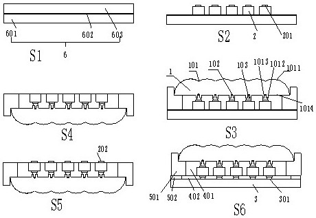
[0036] figure 1 It is a schematic diagram of the manufacturing process of the highly integrated microarray LED packaging module of the embodiment of the present invention, and the specific steps are as follows:

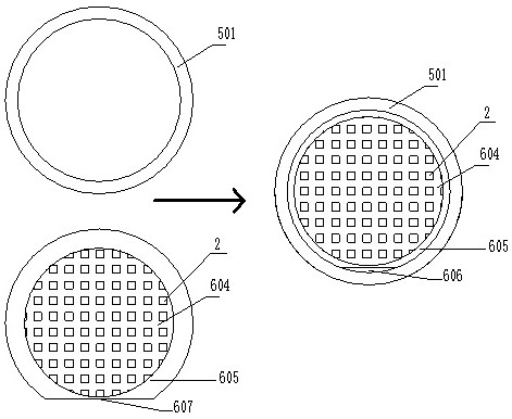
[0037] S1, providing LED prefabricated parts, including microarray lens cover plate 1, epitaxial wafer 6, microarray lens cover plate 1 includes microarray lens 101, metal wiring layer 102 and electrode pad 103; epitaxial wafer 6 includes substrate 601, buffer Layer 602 and epitaxial layer 603. In this embodiment, the size of the epitaxial wafer is preferably 4 inches, that is, the diameter is 100 mm. The edge area of ​​the epitaxial wafer 6 is provided with a mounting area 605. The epitaxial wafer 6 is cleaned ultrasonically by acetone, ethanol or deionized water. surface.

[0038] S2, performing array processing on the epitaxia...


PUM


Abstract

The invention provides a method for manufacturing a high-integration microarray LED packaging module. The method comprises the steps of S1, providing an LED prefabricated part which comprises a microarray lens cover plate and an epitaxial wafer, and cleaning the surface of the epitaxial wafer; S2, carrying out array processing on the epitaxial wafer, wherein the depth of a processed channel reaches a buffer layer, a plurality of chips arranged in an array mode are obtained, and a P electrode is arranged on the surface of the chip; S3, installing the microarray lens cover plate on the epitaxialwafer; S4, inverting the microarray lens cover plate, and performing substrate lift-off on the epitaxial wafer by adopting a laser lift-off process, wherein the lift-off position is the buffer layer;S5, cleaning residues of the buffer layer, processing the surface of the chip, and manufacturing an N electrode; and S6, mounting the microarray lens cover plate on a substrate to obtain the high-integration microarray LED packaging module. The method has the advantages of simple process, good heat dissipation, high integration level and low cost, and has remarkable advantages in the fields of novel illumination, visible light communication and display.

Description

technical field [0001] The invention relates to the field of semiconductor packaging, in particular to a method for manufacturing a highly integrated microarray LED packaging module. Background technique [0002] With the development of LED semiconductor lighting technology, the brightness and lumen density of LED light source have become the main obstacles restricting its large-scale application. Small size, large luminous flux, and uniform luminous microarray LED packaging light source are getting more and more attention in the fields of new lighting, visible light communication and display, and vertical LEDs have more advantages in high-power microarray LEDs. The existing steps for manufacturing vertical LED microarray modules mainly include epitaxial wafer preparation (taking sapphire as an example)-chip production (evaporation-lithography-peeling off substrate or ion distribution-scribing lobes-sorting)-substrate production- Driving electrode fabrication - array extrac...

Claims


Application Information

Patent Timeline
Patent Type & Authority Applications(China)
IPC IPC(8): H01L25/075H01L33/58H01L33/62H01L33/64
CPCH01L25/0753H01L33/58H01L33/62H01L33/642
Inventor 李浩杨私私王晓鹏李峰郝晶龙王好伟
Owner 石家庄费米原科技有限公司
Why Eureka
Try Eureka