Design method of SERS substrate based on surface plasmon polariton effect

A technology of surface plasmons, design methods, applied in nanotechnology for sensing, material excitation analysis, measurement devices, etc.

Active Publication Date: 2020-11-10
HOHAI UNIV CHANGZHOU
View PDF7 Cites 2 Cited by
  • Summary
  • Abstract
  • Description
  • Claims
  • Application Information

AI Technical Summary

Problems solved by technology

Recently, SERS effects have also been found on lithium, sodium, nickel, platinum, palladium, cadmium, merc

Method used


Image

  • Design method of SERS substrate based on surface plasmon polariton effect
  • Design method of SERS substrate based on surface plasmon polariton effect
  • Design method of SERS substrate based on surface plasmon polariton effect

Examples


Embodiment Construction

[0018] The present invention will be further described below in conjunction with the accompanying drawings. The following examples are only used to illustrate the technical solution of the present invention more clearly, but not to limit the protection scope of the present invention.

[0019] A method for designing a SERS substrate based on the surface plasmon effect, comprising the steps of:

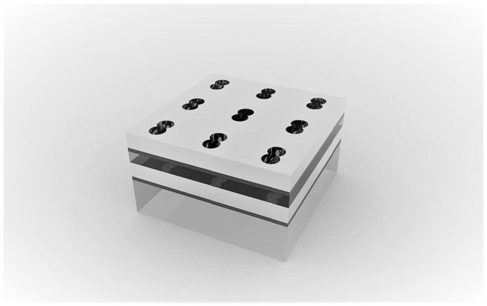
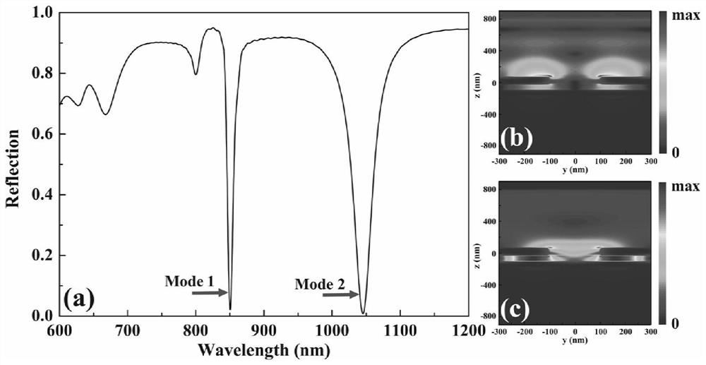
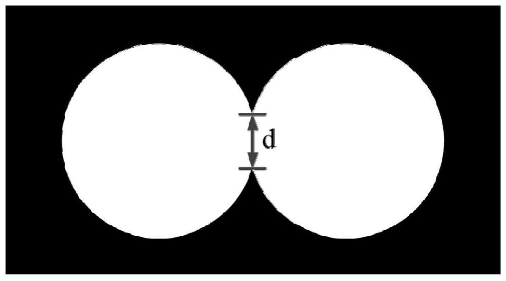
[0020] (1) Using the finite difference time domain algorithm, set the structure of the SERS substrate, which includes SiO 2 base layer, on SiO 2 The base layer is provided with an Au metal film layer, and a layer of SiO is attached on the Au metal film layer. 2 A dielectric layer, on which an Au top layer metal and a double hole structure on the Au top layer metal are arranged, and a periodic boundary structure of the substrate is provided at the same time;

[0021] (2) Determine the initial conditions of the simulation and fix SiO 2 The thickness of the base layer, the boundary con...


PUM


Abstract

The invention discloses a design method of an SERS substrate based on a surface plasmon polariton effect, which comprises the following steps of: setting a structure of an SERS substrate, including aSiO2 substrate layer, an Au metal film layer and a SiO2 dielectric layer, by adopting a time domain finite difference algorithm; determining initial conditions of simulation; sequentially changing thethickness of the Au metal film layer, the thickness of the SiO2 dielectric layer, the thickness of the Au top metal layer and the gap size of the double-circular-hole structure, calculating the electric field intensity distribution of the SERS substrate by utilizing FDTD solution software, calculating an enhancement factor of the SERS substrate according to the electric field intensity distribution, and screening out a structure with a relatively large enhancement factor as the optimized SERS substrate. According to the structure designed by the invention, incident light energy can be effectively converted into surface plasma wave energy, and effective coupling of LSPR and PSPR is generated by etching the composite film SERS substrate of the nano double-hole ordered array, so that an SERSsignal is enhanced to the maximum extent.

Description

technical field [0001] The invention relates to a design method of a SERS substrate based on the surface plasmon effect, and belongs to the technical field of element spectrum analysis enhanced by the surface plasmon effect and SERS. Background technique [0002] Raman spectrum is a kind of scattering spectrum discovered by Indian physicist C.V. Raman in 1928. Like infrared spectrum, it belongs to molecular vibration spectrum, which can reflect various normal vibration frequencies and related vibration levels inside molecules, so that it can Used to identify functional groups present in a molecule. Raman spectroscopy is widely used as a means of analyzing and testing the structure of substances. At present, Raman spectroscopy has been widely used in materials, chemical industry, petroleum, polymer, biology, environmental protection, geology and other fields. However, the Raman scattering effect is a very weak process, and its light intensity is generally only about 10 of t...

Claims


Application Information

Patent Timeline
IPC IPC(8): G01N21/65B82Y15/00B82Y40/00
CPCG01N21/658B82Y15/00B82Y40/00
Inventor 苏巍罗寅龙易恬安陈秉岩
Owner HOHAI UNIV CHANGZHOU
Why Eureka
Try Eureka