Integrated light emitting device

A technology of light-emitting devices and lasers, which is applied in the field of communication, can solve problems such as integration difficulties and high power consumption of light-emitting devices, and achieve the effect of reducing production costs

Inactive Publication Date: 2020-11-27
CHINA ACADEMY OF ELECTRONICS & INFORMATION TECH OF CETC
View PDF5 Cites 3 Cited by
  • Summary
  • Abstract
  • Description
  • Claims
  • Application Information

AI Technical Summary

Problems solved by technology

[0005] The technical problem to be solved by the present invention is to solve the problems of large power consumption and difficult integration of light-emitting devices in the related art. The present invention proposes an integrated light-emitting device

Method used


Image

  • Integrated light emitting device
  • Integrated light emitting device
  • Integrated light emitting device

Examples


Embodiment 1

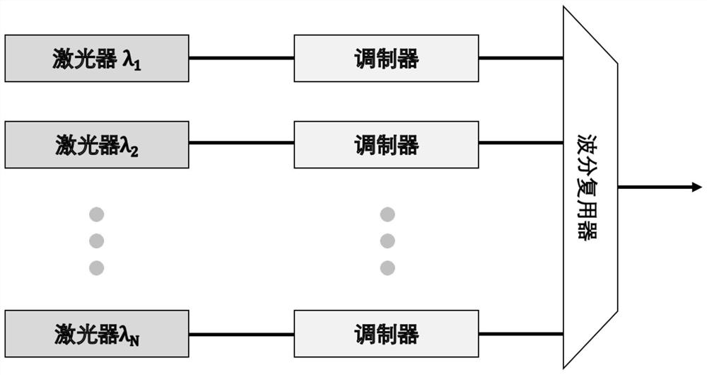
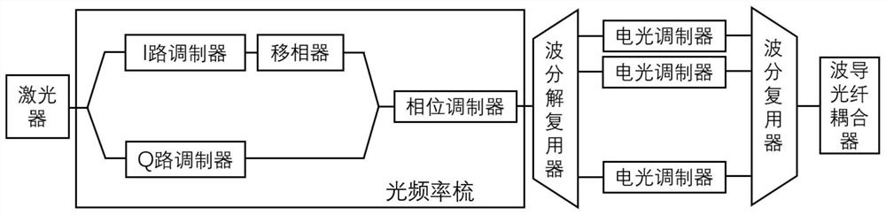
[0079] The optical transmitter of the present invention can be a multi-channel multiplexing silicon-based optical emission chip based on an optical frequency comb, such as image 3 As shown, it mainly includes: semiconductor lasers, silicon-based optical frequency combs, silicon-based wavelength division multiplexers, wave-division multiplexers, silicon-based electro-optic modulators, and electrodes used to control phase shifters in power dividers to drive high-speed The traveling-wave electrode of the electro-optic modulator, the above-mentioned electrode satisfies impedance matching and phase matching, and realizes phase adjustment at high speed and low power consumption.

[0080] Among them, optical frequency combs, electro-optical modulators, wavelength division multiplexers, and wavelength division multiplexers are all fabricated on silicon-on-insulator (SOI) wafers, and the waveguide structure is designed to only satisfy TE mode transmission.

[0081] Such as Figure 4 ...

Embodiment 2

[0103] Such as Figure 18 As shown, the difference from Embodiment 1 is that the silicon-based electro-optic modulator in this embodiment is composed of an IQ modulator, and Figure 4 The structure of the IQ modulator in is the same. V s1 and V s2 The driving signals are respectively loaded to the I-way and Q-way modulators under the same clock. V p1 and V p2 For the phase-shifting voltage of the I-way and Q-way phase shifters, adjust the phase-shifting voltage so that the I-way and Q-way modulators work at the quadrature operating point. Adjust V p3 , so that the I-channel signal and the Q-channel signal are in phase quadrature. The modified modulator can realize high-order code modulation such as QPSK and QAM16. Other structures and obtained effects in this embodiment are the same as those in Embodiment 1.

Embodiment 3

[0105] Such as Figure 19 As shown, the difference from Embodiment 1 is that in this embodiment, there is a thermo-optic phase shifter in the microring resonator cavity in each channel of the silicon-based wavelength division multiplexer, and the thermo-optic effect of silicon can be used to Adjust the resonance point to align the resonance wavelength with the input wavelength, and transmit the light to the bus waveguide to realize wavelength division multiplexing. Wavelength division multiplexing can be realized by exchanging the input and output. Other structures and obtained effects in this embodiment are the same as those in Embodiment 1.

[0106] In addition, the optical transmitter proposed in this application can also use a pulsed mode-locked laser and a micro-ring resonator made of silicon nitride to form an optical frequency comb. The modulator involved in this application can also use a PN junction structure or a PIN junction structure to realize the modulation fun...


PUM


Abstract

The invention provides an integrated light emitting device, which comprises a laser device, an optical frequency comb, a wavelength decomposition demultiplexer and a wavelength division multiplexer which are arranged in sequence in the propagation direction of light, wherein the laser device is used for generating a single-wavelength light source signal; the optical frequency comb is used for receiving the single-wavelength light source signal and processing the signal into a plurality of optical carrier signals with equal wavelength intervals; the wavelength decomposition demultiplexer is used for receiving the multi-wavelength optical carrier signals and decomposing the optical carrier signals into multiple paths of sub-optical carrier signals; and the wavelength division multiplexer isused for combining the multiple paths of sub-optical carrier signals into one path of optical signal and outputting the optical signal. According to the integrated light emitting device, the light source signal is emitted from one laser device, the optical frequency comb receives the light source signal and generates the plurality of carrier signals with equal wavelength intervals to output the light carriers, the problems of high power consumption and difficult temperature control circuit design caused by excessive light emitters are solved, and the production cost of the light emitting device is reduced.

Description

technical field [0001] The invention relates to the technical field of communication, in particular to an integrated light emitting device. Background technique [0002] High-capacity, low-power optical transmission technology is an important means of carrying various data communications. At present, the construction of data centers, 5G communications and backbone networks is facing the problem of faster and faster signal transmission rates and increasing power consumption. Therefore, the optical emission chip is required to have multi-channel capability to increase the transmission rate and reduce chip power consumption to reduce power consumption. Multi-channel parallel emission is an important research direction of optical emission chips in the future, which can effectively increase the transmission rate and reduce the chip size. [0003] In the related art, the main scheme of multi-channel optical emission chip is the direct modulation scheme of vertical cavity surface ...

Claims


Application Information

Patent Timeline
Patent Type & Authority Applications(China)
IPC IPC(8): H04B10/50H04B10/54H04B10/556H04J14/02
CPCH04B10/503H04B10/541H04B10/5561H04J14/02
Inventor 周砚扬李培林张芮闻王鹏飞何立平章宇兵马天琦
Owner CHINA ACADEMY OF ELECTRONICS & INFORMATION TECH OF CETC
Why Eureka
Try Eureka