Chip thin-film resistor network

A thin-film resistor and network technology, which is applied in the direction of thin-film resistors, other resistor networks, resistors, etc., can solve the problem that the temperature coefficient of the thin-film resistor network cannot meet the requirements of use, so as to eliminate vulcanization, reduce damage, and ensure stability. Effect

Pending Publication Date: 2020-12-04
BDS ELECTRONICS
View PDF0 Cites 2 Cited by
  • Summary
  • Abstract
  • Description
  • Claims
  • Application Information

AI Technical Summary

Problems solved by technology

[0003] The purpose of the present invention is to provide a chip type thin film resistance network for the problem that the relative temperature coefficient of the existing thin film resistance network cannot meet the requirements of use.

Method used


Image

  • Chip thin-film resistor network
  • Chip thin-film resistor network
  • Chip thin-film resistor network

Examples


Embodiment 1

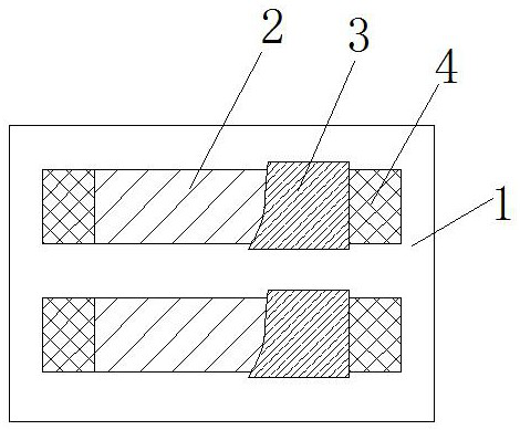
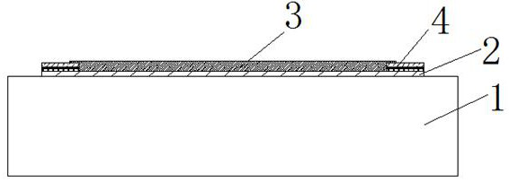
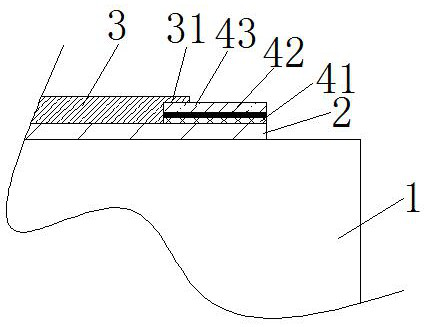
[0029] Such as Figure 1-3 As shown in , a chip-type thin-film resistor network includes a ceramic substrate 1, and a resistive film layer 2 is sputtered on the front of the ceramic substrate 1, and the resistive film layer 2 is a nickel-chromium alloy film, and the resistive film layer 2 is composed of Laser scribing and cutting into individual resistors (eg figure 1 In the figure are two individual resistors), each resistor individual surface is provided with two front electrodes 4 arranged in pairs and separated from each other, the front electrode 4 includes a barrier layer 41, an electrode bottom layer 42 and an electrode surface layer 43 from bottom to top, A passivation layer 3 is provided on the surface of the individual resistor located between the front electrodes 4;

[0030] The barrier layer 41 is a sputtered tungsten-titanium film layer, the electrode bottom layer 42 is a sputtered gold layer, and the electrode surface layer 43 is an electroplated gold layer; the...


PUM

PropertyMeasurementUnit
thicknessaaaaaaaaaa
thicknessaaaaaaaaaa
thicknessaaaaaaaaaa

Abstract

The invention belongs to the technical field of chip thin-film resistors, and particularly relates to a chip thin-film resistor network which comprises a ceramic substrate. A resistive film layer is sputtered on the front surface of the ceramic substrate and is cut into a plurality of resistor units by laser scribing, and two front electrodes are arranged on the surface of each resistor unit. Eachfront electrode comprises a barrier layer, an electrode bottom layer and an electrode surface layer from bottom to top, and a passivation layer is arranged between the front electrodes on the surfaceof each resistor. Compared with the prior art, the chip thin-film resistor network has the advantages that the tungsten-titanium film layer is sputtered to serve as the barrier layer, the stability of the front electrodes can be protected, and a vulcanization phenomenon is eradicated; the processing conditions are controllable, the absolute precision of the resistors of the obtained chip thin-film resistor network reaches + / - 0.05%, a temperature coefficient reaches + / - 5 *10 <6> / K, a relative temperature coefficient reaches + / - 2 *10 <6> / K, and the relative precision reaches + / - 0.02%.

Description

technical field [0001] The invention belongs to the technical field of chip type thin film resistors, and in particular relates to a chip type thin film resistor network. Background technique [0002] Thin-film chip resistors are a new generation of chip resistors with the fastest development, the widest application range and the most promising prospects in recent years. Foreign-funded enterprises began mass production a few years ago, and only a few manufacturers in mainland China can produce this type of resistors. Products, compared with thick film chip resistors, the main component of the resistance film layer of thin film chip resistors is nickel-chromium alloy. After precision machining and post-processing, the resistance value accuracy can reach ±0.5%, and the temperature coefficient can reach ±0.5%. 5ppm / ℃, the stability can reach 0.02%. It is an ideal product to replace low-precision thick-film chip resistors and traditional high-precision, high-stability columnar r...

Claims


Application Information

Patent Timeline
Patent Type & Authority Applications(China)
IPC IPC(8): H01C7/00H01C1/14H01C1/16H01C17/00H01C17/12H01C17/23H01C17/232H01C17/28H01C17/30
CPCH01C1/14H01C1/16H01C7/006H01C17/003H01C17/12H01C17/23H01C17/232H01C17/288H01C17/30
Inventor 徐建建李福喜黄明怀李精喆
Owner BDS ELECTRONICS
Why Eureka
Try Eureka