Rapid ionization device and preparation method thereof

A device and ionization technology, applied in the direction of semiconductor/solid-state device manufacturing, semiconductor devices, electrical components, etc., can solve the problems of long-term stable operation of unfavorable devices, large device on-state loss, high residual voltage, and reduce the range of crossing , The effect of improving the turn-on speed and reducing the residual voltage

Active Publication Date: 2020-12-11
HUAZHONG UNIV OF SCI & TECH
View PDF5 Cites 2 Cited by
  • Summary
  • Abstract
  • Description
  • Claims
  • Application Information

AI Technical Summary

Problems solved by technology

The device design with high resistivity and long base width leads to a high residual voltage at both ends of the device after the FID device is turned on, and a large on-state loss of the device, which is not conducive to the long-term stable operation of the device

Method used


Image

  • Rapid ionization device and preparation method thereof
  • Rapid ionization device and preparation method thereof
  • Rapid ionization device and preparation method thereof

Examples


preparation example Construction

[0044] The present invention also provides the preparation method of described fast ionization device, comprises the following steps:

[0045] (1) Impurity diffusion is performed on the cleaned n-type Si sheet to form a PNP structure; then the p region on one side is removed by a thinning machine to obtain a PN structure comprising a p base region 4 and an n-base region 5;

[0046] (2) Oxidize the PN structure obtained in step (1) to form SiO 2 layer mask layer, remove the SiO on the N side by photolithography 2 A mask layer, forming an n-type ionization-promoting layer 6 on the side of the n-base region through a diffusion process;

[0047] (3) Simultaneously oxidize the upper and lower surfaces of the above-mentioned silicon wafer to form SiO 2 Layer mask layer; through double-sided photolithography, the pattern of the photolithography plate is transferred to the two poles of the Si wafer; the SiO without photoresist protection is removed by etching 2 layer; then remove t...

Embodiment 1

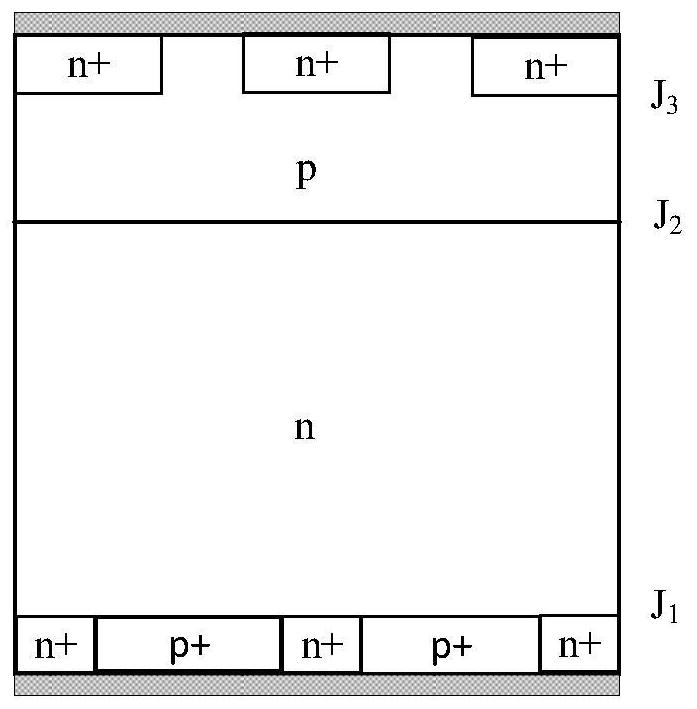
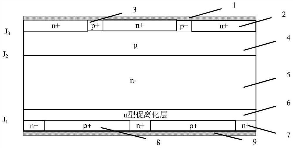
[0061] Such as image 3 As shown, a fast ionization device structure includes: metallized cathode 1, highly doped n+ region 2, highly doped p+ short circuit point 3 on the cathode side, p base region 4, n- base region 5, n-type ionization Layer 6, highly doped n+ short circuit point 7 on the anode side, highly doped p+ region 8, metallized anode 9. The highly doped p+ region 8 is located on the side of the metallized anode 9, and the highly doped n+ short circuit point 7 on the anode side is located between the highly doped p+ regions 8 on the side of the metallized anode 9; the n-type ionization layer 6 is located on the side of the highly doped p+ Layer 8, between the highly doped n+ short-circuit point 7 on the anode side and the n-base region 5, the p-base region 4 is located above the n-base region 5, and the highly-doped n+ region 2 is located between the p-base region 4 and the metallized cathode 1 Between, the highly doped p+ short circuit point 3 on the cathode side ...


PUM

PropertyMeasurementUnit
thicknessaaaaaaaaaa
thicknessaaaaaaaaaa
thicknessaaaaaaaaaa

Abstract

The invention belongs to the field of pulse power semiconductor devices, and particularly relates to a rapid ionization device and a preparation method thereof. The rapid ionization device comprises ametallized cathode, a highly-doped n+ region, a cathode-side highly-doped p+ short-circuit point, a p base region, an n- base region, an n-type ionization promoting layer, an anode-side highly-dopedn+ short-circuit point, a highly-doped p+ region and a metallized anode which are adjacently arranged in sequence. According to the invention, the n-type ionization promoting layer with higher dopingconcentration than the n- base region is introduced into the FID device structure, and the expansion of the space charge region of the n- base region is limited, so that the width of the region to bepenetrated by the collision ionization front edge is limited, the penetration range of the collision ionization front edge is reduced, the propagation time of the collision ionization front edge is shortened, and the reliability of the device is improved, so the switching-on speed of the device is improved.

Description

technical field [0001] The invention belongs to the field of pulsed power semiconductor devices, and more specifically relates to a fast ionization device (FastIonization Dynistor, FID) and a preparation method thereof. Background technique [0002] The delayed avalanche breakdown phenomenon is a new physical phenomenon in semiconductor devices discovered by the Russian Ioffe Research Institute. It reveals that a 10 12 When the reverse voltage is increased by V / s, an ultrafast impact ionization front will be generated inside the device. When the impact ionization front passes through the space charge region of the device, the device will be turned on rapidly. The conduction time of devices designed based on the delayed avalanche breakdown phenomenon can exceed the limit of the saturation drift velocity of free carriers, so that the conduction time of the device can be shortened to the sub-nanosecond range. [0003] Fast ionization device FID is a new type of device based on...

Claims


Application Information

Patent Timeline
Patent Type & Authority Applications(China)
IPC IPC(8): H01L29/06H01L21/822
CPCH01L29/0603H01L29/0684H01L21/822Y02P70/50
Inventor 梁琳黄鑫远
Owner HUAZHONG UNIV OF SCI & TECH
Why Eureka
Try Eureka