
Preparation method of solid film, quantum dot light-emitting device and preparation method

A solid-state film and device technology, applied in semiconductor/solid-state device manufacturing, electrical solid-state devices, semiconductor devices, etc., can solve problems such as poor electronic conductivity

Active Publication Date: 2020-12-18
合肥福纳科技有限公司
View PDF0 Cites 0 Cited by
  • Summary
  • Abstract
  • Description
  • Claims
  • Application Information

AI Technical Summary

Problems solved by technology

In QLED devices, electrons are easier to produce some changes when they are transported in the electron transport layer, which will cause the deterioration of electron conductivity.

Method used


Image

  • Preparation method of solid film, quantum dot light-emitting device and preparation method
  • Preparation method of solid film, quantum dot light-emitting device and preparation method
  • Preparation method of solid film, quantum dot light-emitting device and preparation method

Examples


Embodiment 1

[0058] This embodiment provides a solid-state film and a quantum dot light-emitting device, and the solid-state film is mainly prepared through the following steps:

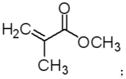
[0059] Mix 0.5mol methyl methacrylate with 100g ZnO nanoparticles, mix evenly, add tetramethylammonium hydroxide solution dropwise to the mixed solution until the solution is clear; form a film on a clean glass substrate by spin coating, The film was then dried at room temperature to obtain a solid film.

[0060] Quantum dot light-emitting devices are mainly prepared through the following steps:

[0061] A hole transport layer, a quantum dot luminescent layer, an electron transport layer, and a cathode are sequentially prepared on a clean glass substrate (containing an anode); wherein, the electron transport layer adopts the above-mentioned preparation method of a solid film.

Embodiment 2

[0063] This embodiment provides a solid-state film and a quantum dot light-emitting device, and the solid-state film is mainly prepared through the following steps:

[0064] Take 0.8mol methyl methacrylate and 100g of TiO 2 The nanoparticles are mixed, and after uniform mixing, ammonia water is added dropwise to the mixed solution until the solution is clear; a film is formed on a clean glass substrate by coating, and then the film is dried at room temperature to obtain a solid film.

[0065] Quantum dot light-emitting devices are mainly prepared through the following steps:

[0066] A hole transport layer, a quantum dot luminescent layer, an electron transport layer, and a cathode are sequentially prepared on a clean glass substrate (containing an anode); wherein, the electron transport layer adopts the above-mentioned preparation method of a solid film.

Embodiment 3

[0068] This embodiment provides a solid-state film and a quantum dot light-emitting device, and the solid-state film is mainly prepared through the following steps:

[0069] Take 0.8mol methyl methacrylate and 100g of TiO 2 The nanoparticles are mixed, and after uniform mixing, ammonia water is added dropwise to the mixed solution until the solution is clear; a film is formed on a clean glass substrate by spin coating, and then the film is dried at room temperature to obtain a solid film.

[0070] Quantum dot light-emitting devices are mainly prepared through the following steps:

[0071] A hole transport layer, a quantum dot luminescent layer, an electron transport layer, and a cathode are sequentially prepared on a clean glass substrate (containing an anode); wherein, the electron transport layer adopts the above-mentioned preparation method of a solid film.


PUM


Abstract

The invention relates to the field of quantum dot light-emitting diodes, in particular to a preparation method of a solid film, a quantum dot light-emitting device and a preparation method. The preparation method of the solid film comprises the following steps of mixing short-chain lipid organic molecules and metal oxide nanoparticles to prepare a mixed solution, and then adding alkali liquor intothe mixed solution until the mixed solution is clarified to obtain a clarified solution, and forming a film from the clarified solution and then curing. Short-chain lipid organic molecules are decomposed into alcohol and acid in the presence of alkali liquor, and hydroxyl in the alcohol and carboxyl in the acid can form hydrogen bonds with hydroxyl, carboxyl, amino, sulfydryl and the like on thesurfaces of the metal oxide nanoparticles. And electron loss caused by combination of hydroxyl, carboxyl, amino, sulfydryl and the like on the surfaces of the metal oxide nanoparticles with electronscan be avoided. The electron transmission performance can be improved. In addition, the hydrogen bonds are beneficial to preventing dehydration reaction on the surfaces of the metal oxide nanoparticles and improving the transmission performance of electrons.

Description

technical field [0001] The present application relates to the field of quantum dot light-emitting diodes, in particular, to a preparation method of a solid film, a quantum dot light-emitting device and a preparation method. Background technique [0002] The problem of charge conductivity of QLED (Quantum Dot Light Emitting Diodes) devices involves two transport layers of charge and holes; among them, the electron transport layer is responsible for transporting electrons from the cathode to the light-emitting layer of the device. In QLED devices, electrons are more likely to produce some changes when they are transported in the electron transport layer, which will cause the deterioration of electron conductivity. Contents of the invention [0003] The purpose of the embodiments of the present application is to provide a method for preparing a solid-state film, a quantum dot light-emitting device and a preparation method, which aim to improve the charge transport performance...

Claims


Application Information

Patent Timeline
IPC IPC(8): H01L51/56H01L51/50
CPCH10K50/115H10K50/16H10K71/00
Inventor 翁兴焕汪鹏生乔之勇
Owner 合肥福纳科技有限公司
Learn More