GaAs-based multi-junction red laser and preparation method thereof

A laser, laser technology, applied in the field of optoelectronics, can solve the problems of limiting the application of semiconductor lasers and poor beam quality, etc.

Active Publication Date: 2020-12-22
Shandong Huaguang Optoelectronics Co. Ltd.
View PDF5 Cites 3 Cited by
  • Summary
  • Abstract
  • Description
  • Claims
  • Application Information

AI Technical Summary

Problems solved by technology

The beam quality of semiconductor lasers is still poor at present, and this shortcoming greatly limits the application of semiconductor lasers. It is widely used in fields such as laser welding that only require low beam quality but require high power.

Method used


Image

  • GaAs-based multi-junction red laser and preparation method thereof

Examples


Embodiment 1

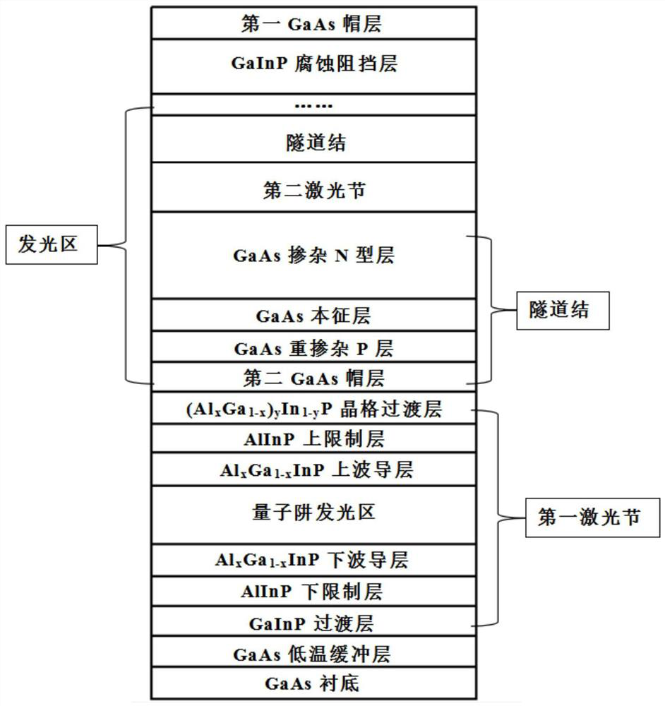
[0100] Step 1: Put the GaAs substrate in the growth chamber of the MOCVD equipment, H 2 The environment is heated to 780°C, baked for 35 minutes, and filled with AsH 3 ;

[0101] Step 2: Slowly lower the temperature to 730°C, continue to feed TMGa and AsH 3 , grow a GaAs low-temperature buffer layer on a GaAs substrate, wherein the thickness of the GaAs low-temperature buffer layer is 200nm, and the doping concentration is 5E17 atoms / cm 3 ;

[0102] Step 3: Slowly lower the temperature to 690°C and continue to feed TMGa, TMIn and PH 3 , a GaInP transition layer is grown on the GaAs low-temperature buffer layer; the doping concentration of the GaInP transition layer is 5E17 atoms / cm 3 ;

[0103] Step 4: Slowly drop the temperature to 660°C, continue to feed TMAl, TMIn and PH 3 , grow an n-type AlInP lower confinement layer on the GaInP transition layer; the thickness of the AlInP lower confinement layer is 0.1um, and the doping concentration is 1E17 atoms / cm 3 ;

[0104...

Embodiment 2

[0120] Step 1: Put the GaAs substrate in the growth chamber of the MOCVD equipment, H 2 The environment is heated to 800°C, baked for 35 minutes, and filled with AsH 3 ;

[0121] Step 2: Slowly lower the temperature to 730-770°C, continue to feed TMGa and AsH 3 , grow a GaAs low-temperature buffer layer on a GaAs substrate, wherein the thickness of the GaAs low-temperature buffer layer is 800nm, and the doping concentration is 6E17 atoms / cm 3 ;

[0122] Step 3: Slowly lower the temperature to 710°C and continue to feed TMGa, TMIn and PH 3 , a GaInP transition layer is grown on the GaAs low-temperature buffer layer; the doping concentration of the GaInP transition layer is 3E18 atoms / cm 3 ;

[0123] Step 4: Slowly drop the temperature to 680°C, continue to feed TMAl, TMIn and PH 3 , grow the n-type AlInP lower confinement layer on the GaInP transition layer; the thickness of the AlInP lower confinement layer is 2um, and the doping concentration is 8E17 atoms / cm 3 ;

[0...

Embodiment 3

[0140] Step 1: Put the GaAs substrate in the growth chamber of the MOCVD equipment, H 2 The environment is heated to 820°C, baked for 35 minutes, and filled with AsH 3 ;

[0141] Step 2: Slowly drop the temperature to 770°C, continue to feed TMGa and AsH 3 , grow a GaAs low-temperature buffer layer on a GaAs substrate, wherein the thickness of the GaAs low-temperature buffer layer is 1500nm, and the doping concentration is 6E18 atoms / cm 3 ;

[0142] Step 3: Slowly lower the temperature to 690-730°C, and continue to feed TMGa, TMIn and PH 3 , grow a GaInP transition layer on the GaAs low-temperature buffer layer; the doping concentration of the GaInP transition layer is 5E18 atoms / cm 3 ;

[0143] Step 4: Slowly drop the temperature to 700°C, continue to feed TMAl, TMIn and PH 3 , grow the n-type AlInP lower confinement layer on the GaInP transition layer; the thickness of the AlInP lower confinement layer is 4um, and the doping concentration is 5E18 atoms / cm 3 ;

[0144...


PUM

PropertyMeasurementUnit
thicknessaaaaaaaaaa
thicknessaaaaaaaaaa
thicknessaaaaaaaaaa

Abstract

The invention discloses a GaAs-based multi-junction red laser and a preparation method thereof, the GaAs-based multi-junction red laser comprises a GaAs substrate, a GaAs low-temperature buffer layer,a first laser section, a GaInP corrosion barrier layer and a first GaAs cap layer are sequentially grown on the GaAs substrate from bottom to top, and a plurality of light-emitting layers are grown on the first laser section and the GaInP corrosion barrier layer; each light-emitting layer comprises a plurality of tunnel junctions and a second laser section from bottom to top, the tunnel junctionclosest to the first laser section grows on the first laser section, and the second laser section grows on the tunnel junction; according to the invention, through the design of the tunnel junction, the growth of a multi-section laser material is realized, higher output power is obtained under lower current, and the luminous power of the laser is improved; meanwhile, due to the fact that the interface broadband between the AlInP upper limiting layer and the second GaAs cap layer is discontinuous, the (AlxGa1x)yIn1yP lattice transition layer is introduced in the technical scheme, the voltage isreduced, the reliability of the device is improved, the service life of the device is prolonged, and high practicability is achieved.

Description

technical field [0001] The invention relates to the technical field of optoelectronics, in particular to a GaAs-based multi-junction red laser and a preparation method thereof. Background technique [0002] Semiconductor lasers, also known as laser diodes (LD), use the optical oscillations generated by the stimulated emission of photons caused by semiconductor electron optical transitions to emit laser light. From the development of its structure, it can be roughly divided into the following stages: the initial homojunction laser; the double heterojunction laser that realizes continuous lasing at room temperature; the quantum well laser that greatly improves the performance of semiconductor lasers; further Development of strained quantum well lasers. [0003] Due to the splitting of energy levels in the quantum well active region, the electronic energy state density of the conduction band is greatly increased, and the population inversion is more likely to occur. Therefore,...

Claims


Application Information

Patent Timeline
Patent Type & Authority Applications(China)
IPC IPC(8): H01S5/323
CPCH01S5/32316H01S5/32325
Inventor 李志虎张新朱振于军
Owner Shandong Huaguang Optoelectronics Co. Ltd.
Why Eureka
Try Eureka