Photodetector
A photodetector and photocurrent detection technology, which is applied in the direction of instruments, optics, light guides, etc., can solve the problems of falling defective products and uneven light receiving performance
- Summary
- Abstract
- Description
- Claims
- Application Information
AI Technical Summary
Problems solved by technology
Method used
Image

Examples
Embodiment 1
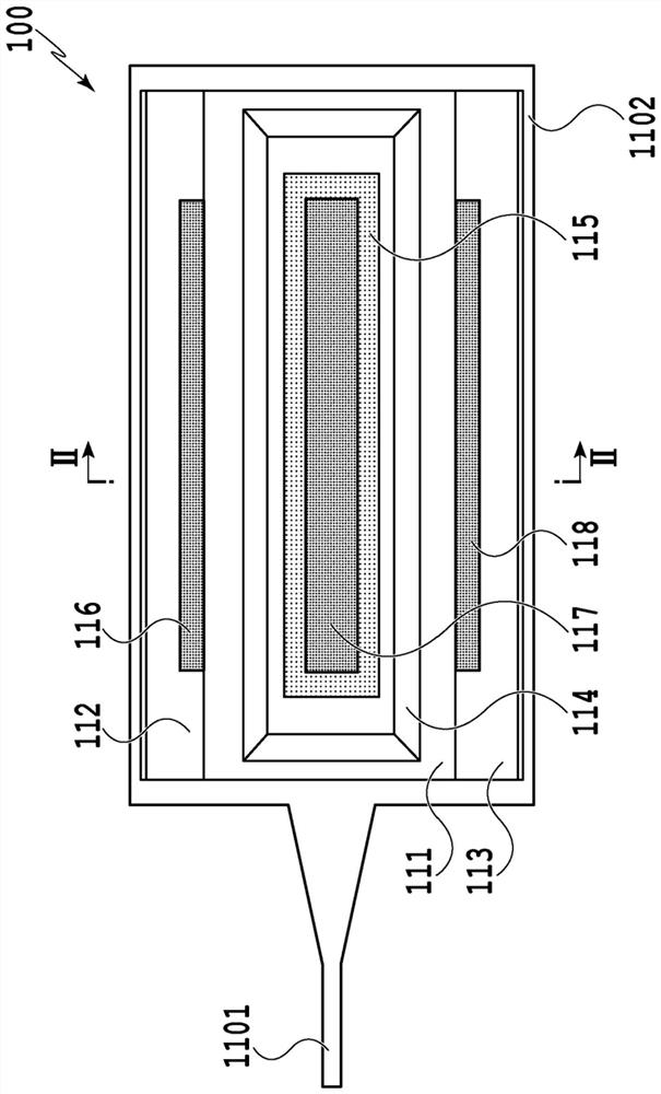
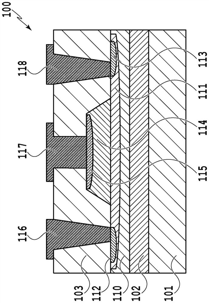
[0063] Figure 4 It is a plan view schematically showing a chip structure of a GePD400 according to Structural Example 1 of Example 1 of the photodetector of the present invention. Figure 5 yes Figure 4 The cross-sectional view of the V-V plane (the plane perpendicular to the direction of light travel) of .
[0064] Figure 4 and Figure 5 The GePD 400 of the shown structure example 1 includes, for example, a Si substrate 401, a lower cladding layer 402 including a Si oxide film, a silicon core layer 410 for guiding signal light to be detected, and a substrate for transmitting the signal light from the substrate to the same SOI structure as conventional ones. The input waveguide 4101 that guides the wave toward the silicon core layer in the in-plane direction is formed on the semiconductor substrate.
[0065] On the region of the silicon plate 4102 of the silicon core layer 410 of the semiconductor substrate, a Ge layer 414 constituting a light absorbing layer is provide...
Embodiment 2
[0093] Figure 15 It is a diagram showing the configuration of the optical circuit of the second embodiment in which the photodetector in the first embodiment is mounted on a coherent optical transmitter having a polarization diversity configuration. Figure 15 It shows: an optical power splitter 801, which branches the transmission carrier light from the light source; a Y polarization modulation circuit 802 and an X polarization modulation circuit 803, which use electrical signals for each polarization to branch the transmission carrier light light modulation; the polarization rotator 808, which rotates the polarization of one polarized light to the other; and the polarization beam combiner 809, which serves as a polarization separation / combination circuit for combining modulated lights of each polarization.
[0094] as Figure 15 The power monitoring configuration of the coherent optical transmitter of the present invention branches off a part of the optical output of the X...
Embodiment 3
[0096] Figure 16 It is a diagram showing the configuration of the optical circuit of Example 3 in which the photodetector in Example 1 is mounted on a coherent optical receiver having a polarization diversity configuration.
[0097] Figure 16 shows the optical input path 901 of the reference light from the local oscillator light source, the input path 902 from the input port of the received signal light, the polarization beam splitter 903 as a polarization splitting / combining circuit for polarization splitting the received signal light, Polarization rotator 904 . Figure 16 It also shows the optical power splitter 909 for optical branching, the optical coherent mixer 910 for Y polarization demodulation, the optical coherent mixer 911 for X polarization demodulation, and the conversion of the demodulated optical signal PD912, 913 for electrical signals.
[0098] In addition, as a configuration for monitoring the power of received light, Figure 16 Shown are monitoring opt...
PUM
 Abstract
Description
Claims
Application Information
 - R&D
- Intellectual Property
- Life Sciences
- Materials
- Tech Scout
- Unparalleled Data Quality
- Higher Quality Content
- 60% Fewer Hallucinations
Browse by: Latest US Patents, China's latest patents, Technical Efficacy Thesaurus, Application Domain, Technology Topic, Popular Technical Reports.
© 2025 PatSnap. All rights reserved.Legal|Privacy policy|Modern Slavery Act Transparency Statement|Sitemap|About US| Contact US: help@patsnap.com