PN junction gate-controlled gallium oxide field effect transistor and preparation method thereof

A gallium oxide field and transistor technology, applied in semiconductor/solid-state device manufacturing, semiconductor devices, electrical components, etc., can solve the constraints on the development and application of gallium oxide-based devices, the easy passivation activation rate of acceptor impurity ions, and the lack of shallow energy Eliminate the self-heating effect, high lattice integrity and low cost

Inactive Publication Date: 2021-01-01
XIDIAN UNIV
View PDF6 Cites 2 Cited by
  • Summary
  • Abstract
  • Description
  • Claims
  • Application Information

AI Technical Summary

Problems solved by technology

Compared with n-type doping of gallium oxide crystals, p-type doping is more difficult to achieve, especially p-type doping with higher carrier concentration
The main reasons why it is difficult to obtain effective p-type doping are: the influence of n-type background carriers; the lack of effective shallow-level acceptor impurities; the acceptor impurity ions are easy to passivate and the activation rate is low, and there is a self-defect effect
Therefore, research on gallium oxide-based devices is also mainly focused on n-type β-Ga 2 o 3 Based devices, there are few research results on p-type conductive single crystal, thin film and p-type channel devices, which restricts the development and application of gallium oxide-based devices. Bipolar devices widely used in commercial Si and SiC power electronic devices structures and junction-based edge termination structures, which are quite challenging for GaO-based devices
In addition, circuits composed of normally-off devices can be powered by a single power supply. This feature simplifies the circuit, increases the reliability of the circuit, and has low static loss. However, most of the existing n-type GaO devices need to be powered by a certain Negative gate voltage can be turned off, which limits the application range of the device

Method used


Image

  • PN junction gate-controlled gallium oxide field effect transistor and preparation method thereof
  • PN junction gate-controlled gallium oxide field effect transistor and preparation method thereof

Examples


Embodiment 1

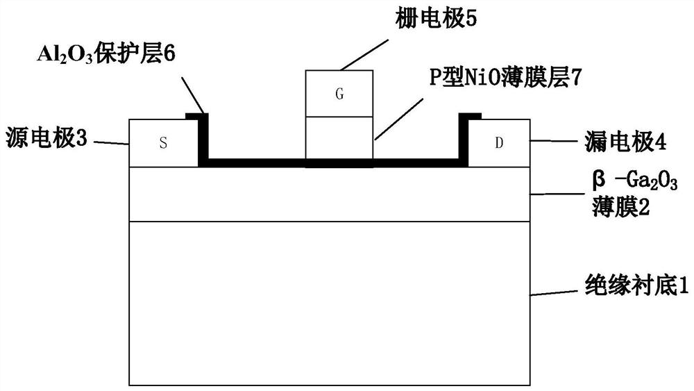
[0032] Embodiment 1, making insulating substrate is SiO 2 / p + -Si, n-type β-Ga 2 o 3 Gallium oxide field effect transistor with film thickness of 100nm and p-type NiO film thickness of 200nm.

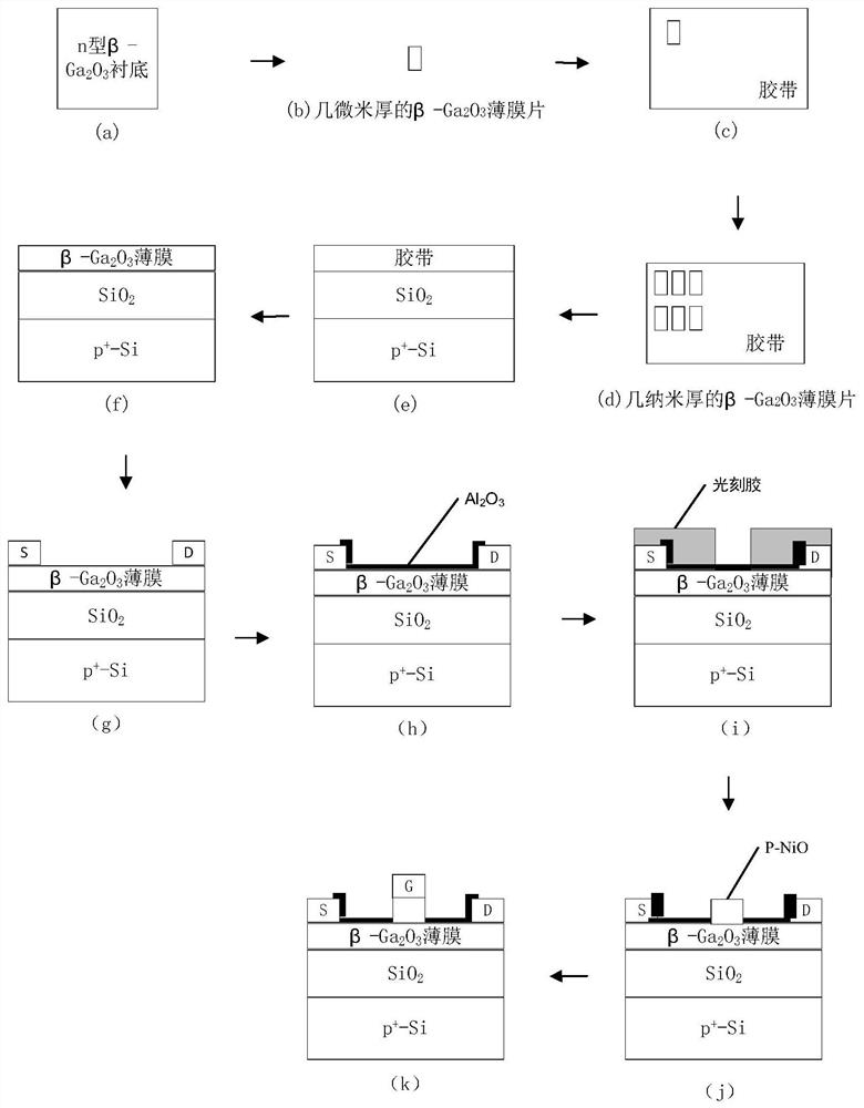
[0033] Step 1: Cleaning β-Ga 2 o 3 single crystal substrates, such as figure 2 (a).

[0034] Select the doping concentration as 2.7e18cm -3 n-type β-Ga 2 o 3 The single crystal substrate was then ultrasonically cleaned in acetone solution, absolute ethanol, and deionized water for 5 min each, and then dried with nitrogen.

[0035] Step 2: Prepare β-Ga with a thickness of micrometers by mechanical exfoliation 2 o 3 film.

[0036] Due to β-Ga 2 o 3 The bonding force between the crystal (100) planes is weak, so the mechanical exfoliation method is used, and the n-type β-Ga after cleaning 2 o 3 Cleave the crystal along the (100) plane with a blade or tweezers on the single crystal substrate to obtain micron-sized β-Ga 2 o 3 film, such as figure 2 (b);

[0037] The pre...

Embodiment 2

[0055] Embodiment 2, making the insulating substrate is sapphire, n-type β-Ga with a thickness of 300nm 2 o 3 Gallium oxide field effect transistor with film thickness of 100nm and p-type NiO film thickness of 300nm.

[0056] Step 1: Cleaning β-Ga 2 o 3 single crystal substrates, such as figure 2 (a).

[0057] 1.1) Select the doping concentration to be 3e18cm -3 n-type β-Ga 2 o 3 single crystal substrate;

[0058] 1.2) The selected n-type β-Ga 2 o 3 The single crystal substrate was ultrasonically cleaned in acetone solution, absolute ethanol, and deionized water for 5 min each, and then dried with nitrogen.

[0059] Step 2: Prepare β-Ga with a thickness of micron order by mechanical exfoliation 2 o 3 film.

[0060] 2.1) According to β-Ga 2 o 3 The crystal (100) has a weak interplanetary bonding force, and the mechanical exfoliation method is used to clean the n-type β-Ga 2 o 3 Cleave the crystal along the (100) plane with a blade or tweezers on the single cryst...

Embodiment 3

[0083] Embodiment 3, making the insulating substrate is sapphire, n-type β-Ga with a thickness of 200nm 2 o 3 Gallium oxide field effect transistor with film thickness of 75nm and p-type NiO film thickness of 150nm.

[0084] Step A: Cleaning β-Ga 2 o 3 single crystal substrates, such as figure 2 (a).

[0085] First, choose a doping concentration of 1e18cm -3 n-type β-Ga 2 o 3 single crystal substrate;

[0086] Then, the selected n-type β-Ga 2 o 3 The single crystal substrate was ultrasonically cleaned in acetone solution, absolute ethanol, and deionized water for 5 min each, and then dried with nitrogen.

[0087] Step B: Prepare micron-scale β-Ga by mechanical exfoliation 2 o 3 film.

[0088] First, using the mechanical stripping method, the cleaned n-type β-Ga 2 o 3 Cleave the crystal along the (100) plane with a blade or tweezers on the single crystal substrate to obtain micron-sized β-Ga 2 o 3 film, such as figure 2 (b);

[0089] Then, the prepared micr...


PUM

PropertyMeasurementUnit
thicknessaaaaaaaaaa
etching poweraaaaaaaaaa
thicknessaaaaaaaaaa

Abstract

The invention discloses a PN junction gate-controlled gallium oxide field effect transistor and a preparation method thereof, and mainly solves the problems of effective p-type doping of a gallium oxide material and bipolar structure loss of a gallium oxide-based device at present. The transistor comprises an insulating substrate and an n-type beta-Ga2O3 thin film layer from bottom to top, a source electrode and a drain electrode are arranged at the two ends of the n-type beta-Ga2O3 thin film layer, a gate electrode is arranged in the middle area, and Al2O3 protection layers are arranged on the n-type beta-Ga2O3 thin film layer between the gate electrode and the source electrode and between the gate electrode and the drain electrode and on the inner surfaces of the source electrode and thedrain electrode. A p-type NiO thin film layer is arranged between the n-type beta-Ga2O3 thin film layer and the gate electrode, and the p-type NiO thin film layer and the n-type beta-Ga2O3 thin filmform a p-n junction. According to the invention, the on-resistance and the gate leakage current of the device are reduced, the voltage endurance capability of the device is improved, the static loss of the device is reduced, and the method can be used for preparing a normally-off high-voltage-withstanding gallium oxide device.

Description

technical field [0001] The invention belongs to the technical field of semiconductor devices, and in particular relates to a PN junction gate-controlled gallium oxide field effect transistor, which can be used to prepare a normally-off high-voltage gallium oxide device. [0002] technical background [0003] Gallium oxide has five crystal forms of α, β, γ, δ and ε, among which the monoclinic β-Ga 2 o 3 With the best thermal stability, other metastable phases can easily transform into β-Ga at high temperature 2 o 3 , so most of the current research is around β-Ga 2 o 3 Expanded. β-Ga 2 o 3 It has a large forbidden band width (4.4-4.9eV), which makes its ionization rate low and the breakdown field strength is high, about 8MV / cm, which is more than 20 times that of Si and twice that of SiC and GaN many. In addition, β-Ga 2 o 3 The quality factor of Baliga is more than 8 times that of 4H-SiC and more than 4 times that of GaN; the high-frequency Baliga figure of merit i...

Claims


Application Information

Patent Timeline
Patent Type & Authority Applications(China)
IPC IPC(8): H01L29/808H01L21/337H01L29/06H01L29/24
CPCH01L29/8086H01L29/66924H01L29/0611H01L29/0665H01L29/24
Inventor 周弘雷维娜周昕张进成郝跃
Owner XIDIAN UNIV
Why Eureka
Try Eureka